Design and Implementation of a Digital Lock
(Finite State Machine Lab)
Purpose
The purpose of this lab is:
You need to design a digital lock that has three input push-buttons: A, B and C. Assume that the buttons cannot be pressed simultaneously (an electromechanical interlock guarantees this). The lock should have the following features:
2. Once the lock is open, one can close the lock by pressing any key.
3. To reset the lock to its initial state one can press the sequence A-A from any state, except the alarm state or the reset state.
4. In order to prevent tampering with the lock, an ALARM will go off after pressing a wrong button. However, in order to make it harder to figure out the right sequence, we don't want the alarm to go off after the first wrong button has been pressed. Instead, the alarm should go off after pressing 4 buttons, as long as one of the 4 buttons pressed is a wrong one (e.g. the sequences B-C-B-A, A-B-C-A, C-C-B-A, A-A-B-C, etc. would trigger the alarm).
5. The only way to get out of the alarm state is by pressing the C-A
sequence.
Task one: Design of the Digital Lock FSM.
2. Draw the state diagram or ASM (Algorithmic State Machine) chart for the digital lock. If you make assumptions because not everything was specified, write them down. Indicate what each state represents, what input conditions cause the state transitions, and what the corresponding outputs are. Number the state S0, S1, etc. The digital lock should have as outputs the UNLOCK and ALARM signals. In order to follow the operation of the FSM during testing, you will also show in the 7-segment display the number of the state that is active. The state that corresponds to the UNLOCK and ALARM situation should be displayed as "U" and "A". It would be great is you could have the "A" blinking to draw the attention that the alarm has been set off. I would suggest to design the state diagram as a Moore machine since that makes the timing easier.
3. After you have derived the state diagram, review the section on "State Editor" , Behavioral Description VHDL or "State Diagrams" in the ABEL-HDL tutorial.
As part of this task you will be concentrating on implementing and testing your design. This raises some interesting issues which are mainly related to timing. In your design you have assumed that when you press the push-button it will generate a single pulse which is synchronized with the clock. In reality this is not going to be the case unless you take special precautions. We are concerned with three issues:
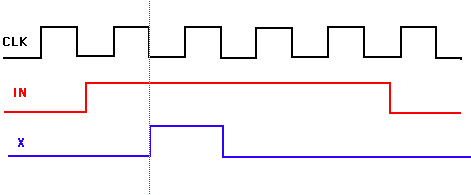
2. A second problem comes from the fact that when one presses the push-button for a short moment, the time that the switch will be closed is usually much longer (msec range) than one clock period (microseconds or even nanoseconds). As a result, our digital lock (or any other finite state machine) will think that we are supplying a string of ones as the input. Thus, one needs to add a circuit after each push-button switch that will generate only one pulse every time that one presses the push-button, independent of the time one keeps the button pressed. Figure 1 shows the timing diagram.
Figure 1: Timing diagram: signal IN is generated asynchronously while signal X is a pulse that is in sync with the clock signal and lasts for only one clock period.
Notice that in Figure 1 the pulse X is synchronized with the falling
edge of the clock. If one uses this pulse as the input to a finite state
machine (or FF) that is clocked at the positive clock edge, one has ensured
that the set-up and hold times will be respected.
The overall digital lock system is shown in Figure
2. It consists of the core FSM for the lock, together with the debouncing
and one-pulse circuit for each push button input. The 7-segment LED is
used to display the number of each state or the Alarm (A) and Unlock (U)
states.
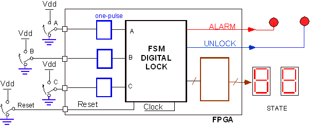
Figure 2: Schematic Block diagram of the Digital Lock system.
Design a circuit that generates a single pulse independent of the length of the input signal IN. You can assume that the clock period is much shorter than the time the input signal IN is asserted high. There are different methods to design such a circuit. One is an ad-hoc method where you are using your experience with flip-flops to come up with the circuit. An alternative method is more systematic and makes use of finite state machine design method. Indeed, the circuit we need to come up with can be considered as a finite state machine with one input and one output. In case you prefer the last method, you should give the state diagram, (or ASM), the transition table, the next state logic (assuming that you are using D flip-flops) and the schematic (flip-flops and gates). Notice that this circuit also takes care of the synchronization problem discussed above.
In summary, you need to design the following circuits as part of the pre-lab:
In-lab assignment:
A. Parts and Equipment:
The goal is to implement, download, display and test the digital lock whose block diagram is shown in Figure 2. During the first task you will design and simulate the finite state machines of the digital lock and the synchronization (one-pulse) circuit. You will also design and simulate the debouncing circuit. As part of the second task, you will complete the top level schematic, simulate, and debug the overall circuit. Finally, you need to compile (implement) and download the circuit on an FPGA or CPLD and test its operation. A demo needs to be given to the lab instructors..
Task one: Design of the digital lock FSM and a one-pulse circuit.
2. Design the Finite State machine for the digital lock using the State Editor, or by writing the HDL code based on the state diagram or algorithmic state machine you derived as part of the pre-lab.
3. Simulate the macro to verify the proper operation of the digital lock.
2. Simulate the top level schematic and verify that the overall
circuit works properly. Debug if necessary.
3. When successful, take a screen capture of the functional simulation illustrating the proper operation.
2. After the translation, you can use the constraint editor to define the pin locations. Alternatively you can place the pin location on the schematic as you did in the first lab.
3. When done with the constraint editor, you can invoke the interactive
flow engine to implement the circuit using the new constraint file (make
sure you are using the right file as explained in the Constraint Editor
write-up). Check the Pad report everytime you run the implementation and
verify that the pads have been assigned to the right pin numbers.
In case you have difficulties assigning the right pin numbers with the
contraint editor, edit
the user constraint file).
4. If the implementation was successful, check the Map Report for the device utilization and the Post Layout Timing Report.
5. Download the circuit.
6. Check the operation of the Digital Lock and observe the UNLOCK, ALARM and State signals. Check as many possible key sequences as possible to convince yourself that the lock works properly under all conditions. Check for instance following sequences (write this in your lab notebook and write down the results of the tests).:
If the system does not work properly check your state diagram and
other circuits. Check also the pad reports to make sure that the right
pin locations have been assigned. In case you are using the XS40
board and the system is circulating through different states, this indicates
that the pullup resistors were not implemented. Go back to the schematic
and check that the pullup resistors have been placed properly between the
input pad and the input buffer. Before closing the schematic, go to OPTION
-> CREATE NETLIST. Implement the circuit again and download the latest
version/revision. When the circuit works successfully, give a demo to
the lab instructor.
7. Take a screen capture of the top level schematic, and the schematics or HDL code for each macro.
Hand-in
You must hand in a lab report that contains the following:
2. Section on the Pre-lab with answers to all questions.
3. Section on the lab experiment:
b. Copy of the schematics (screen capture) and HDL source code of each macro (screen capture)
c. Simulation results
d. Summary of the Device utilization and the delays.
e. Discussion of the results indicating that the circuit functions properly.
1. M. Mano and C. Kime, "Logic anc Computer Design Fundamentals," 2nd
Edition, Prentice Hall, Upper Saddle River, NJ, 2001.
2. R. Katz, "Contemporary Logic Design", Benjamin/Cummings Publ., Reading,
MA, 1994.
3. J. F. Wakerly, "Digital Design," 3rd edition, Prentice Hall, Upper
Saddle River, NJ, 2000.
4. P. Horowitz and W. Hill, "The Art of Electronics", Cambridge University
Press, Cambridge, 1989; p506.
5. XILINX XC4000
FPGA description.
Copyright, 1999 Jan Van der Spiegel; Created by Jan Van der Spiegel; November 14, 1997; Updated November 14, 2001.