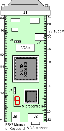
|
CHIP PIN No.
|
XC95108 Pin Name
|
XS95 board connection
|
|
1
|
I/O |
A4 (Address bit of the SRAM) |
|
2
|
I/O |
A7 (Address bit of the SRAM) |
|
3
|
I/O |
A5 (Address bit of the SRAM) |
|
4
|
I/O |
Free I/O 0 |
|
5
|
I/0 |
P1.3 |
|
6
|
I/O |
P1.0 (Port 1 of the microcontroller) and PC parallel port Control Output
C0 |
|
7
|
I/O |
P1.1 |
|
8
|
GND |
|
|
9
|
I/O /GCK1(Global CLK1) |
CLK (from Programmable oscillator) |
|
10
|
I/O /GCK2 |
Output clock generated by the CPLD, connected to the clock input XTAL1
of the microcontroller. |
|
11
|
I/O |
P1.2 |
|
12
|
I/O /GCK3 |
Free I/O 1 |
|
13
|
I/O |
PSEN (program store enable) |
|
14
|
I/O |
7-segment disp.-f (S5)/ Red1of VGA |
|
15
|
I/O |
7-segment disp.-a (S6)/Hor SYNC of VGA |
|
16
|
GND |
|
|
17
|
I/O |
7-segment disp.-g (S3)/ Green1of VGA |
|
18
|
I/O |
7-segment disp.-b (S4)/ Red0 of VGA |
|
19
|
I/O |
7-segment disp.-e (S2)/ Green0 of VGA |
|
20
|
I/O |
ALE (address latch enable pin) |
|
21
|
I/O |
7-segment disp.-d (S0)/Blue0 of VGA |
|
22
|
VCC |
|
|
23
|
I/O |
7-segment disp.-c (S1)/ Blue1 of VGA |
|
24
|
I/O |
7-segment disp. - dec. pt/ Vert. SYNC of the VGA |
|
25
|
I/O |
Free I/O 2 |
|
26
|
I/O |
P3.4 (T0 - Timer 0) and KB_CLK of PS/2 |
|
27
|
GND |
|
|
28
|
TDI (Test data
in - for boundary scan) |
P2.7( A15): Port P2.7 of microcontroller and addr. bit A15 of SRAM
(only on the 128KB) |
|
29
|
TMS (test
mode) (for boundary scan) |
ALE (address latch enable pin) |
|
30
|
TCK (Test clock
- for boundary scan) |
|
|
31
|
I/O |
P3.0 (RXD) |
|
32
|
I/O |
P3.7 (/RD) |
|
33
|
I/O |
P3.5 (T1 - timer 1) |
|
34
|
I/O |
P2.7(A15).A15 |
|
35
|
I/O |
P0.7(AD7)/D7 (multiplexed address/data port and also conntected to
data pin D7 of SRAM) |
|
36
|
I/O |
P0.6(A.D6)/D6 |
|
37
|
I/O |
P0.5(A.D5)/D5 |
|
38
|
VCC |
|
|
39
|
I/O |
P0.4(AD4)/D4 |
|
40
|
I/O |
P0.3(AD3)/D3 |
|
41
|
I/O |
P0.2(AD2)/D2 |
|
42
|
GND |
|
|
43
|
I/O |
P0.1(AD1)/D1 |
|
44
|
I/O |
P0.0(AD0)/D0 |
|
45
|
I/O |
RST (reset input of the microconroller) |
|
46
|
I/O |
Parallel port data output PC-D0 (can be used for
clock signals - has an inverting Schmitt-trigger) |
|
47
|
I/O |
Parallel port data output PC-D1 (can be used for clock
signals - has an inverting Schmitt-trigger) |
|
48
|
I/O |
Parallel port data output PC-D2 |
|
49
|
GND |
GND |
|
50
|
I/O |
Parallel port data output PC-D3 |
|
51
|
I/O |
Parallel port data output PC-D4 |
|
52
|
I/O |
Parallel port data output PC-D5 |
|
53
|
I/O |
P2.4(A12)/A12 (Port P2.4 of microcontroller and addr. bit A12 of SRAM |
|
54
|
I/O |
P2.2(A10)/A10 |
|
55
|
I/O |
P2.3(A11)/A11 |
|
56
|
I/O |
P2.1(A9).A9 |
|
57
|
I/O |
P2.5 (A13)/A13 |
|
58
|
I/O |
P2.0(A8)/A8 |
|
59
|
TDO |
|
|
60
|
GND |
|
|
61
|
I/O |
P2.6 (A14)/A14 |
|
62
|
I/O |
/OE (SRAM output enable pin) |
|
63
|
I/O |
P3.6 (/WR - data write) and /WE of SRAM |
|
64
|
VCC |
|
|
65
|
I/O |
/CE (SRAM chip enable) |
|
66
|
I/O |
P1.6 and parallel port PC-S5 |
|
67
|
I/O |
P1.7 |
|
68
|
I/O |
P3.3 (/INT1 - interrupt1) |
|
69
|
I/O |
P3.2 (/INT0 - interrupt0) |
|
70
|
I/O |
P3.1 (TXD), parallel Port PC-S6, KB_Data of PS/2 port |
|
71
|
I/O |
P1.5 and parallel port PC-S3 |
|
72
|
I/O |
P1.4 and parallel port PC-S4 |
|
73
|
VCC |
|
|
74
|
I/O |
A16 (Addr bit of SRAM) (For 128KB version) |
|
75
|
I/O |
A0 (Addr. bit of SRAM) |
|
76
|
I/O |
Free I/O 3 |
|
77
|
I/O |
Free I/O 4 |
|
78
|
VCC |
5V |
|
79
|
I/O |
A1 (SRAM) |
|
80
|
I/O |
Parallel port data output PC-D7 |
|
81
|
I/O |
Parallel port data output PC-D6 |
|
82
|
I/O |
A2 (SRAM) |
|
83
|
I/O |
A6 (SRAM) |
|
84
|
I/O |
A3 (SRAM) |