Figure 1: Addition of binary numbers
Full Adder Lab
Introduction to the Xilinx Foundation System -
Schematic entry, Functional Simulation and Implementation
Purpose:
The purpose of this lab is:
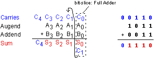
The Half Adder of the previous lab adds two bits and generates a Sum and Carry-out output. However, to be useful for adding binary words, one needs a Full Adder (FA) which has three inputs: the augend, the addend, and a Carry-in. The following example illustrates the addition of two 4-bit words A(A3A2A1A0) and B(B3B2B1B0).
Figure 1: Addition of binary numbers
The addition can be split-up in bit slices. Each slice performs the addition of the bits Ai, Bi and the Carry-in bit Ci (= Carry-out bit of the previous slice). Each slice consists of a full adder, illustrated below.
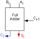
Figure 2: Block diagram of a full adder (FA)
A circuit that implements a full adder is given in Figure 3 below.
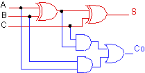
Figure 3: Logic diagram of a Full Adder
The circuit consists of two XOR gates, two AND gates and one OR gate.
The XOR=AÅB, also called exclusive OR,
is defined by the following truth table.
|
|
|
|
|
|
|
|
|
|
|
|
|
|
|
|
|
|
|
|
|
|
|
|
Pre-lab assignment:
Before coming to the lab read the pre-lab section and answer all the questions. Write the derivations down in your lab notebook. See guidelines on keeping a notebook. Failing to do the pre-lab in advance will make it impossible to finish the actual lab on time.
| Inputs | Outputs | |||
| A | B | C | Sum | Co |
| 0 | 0 | 0 | . | . |
| 0 | 0 | 1 | . | . |
| 0 | 1 | 0 | . | . |
| 0 | 1 | 1 | . | . |
| 1 | 0 | 0 | . | . |
| 1 | 0 | 1 | . | . |
| 1 | 1 | 0 | . | . |
| 1 | 1 | 1 | . | . |
3. Verify that the expressions for S and Co derived above correspond to the outputs defined in the truth table of question 1. Check for the 8 possible combintations of the input signals and write down the corresponding outputs S and Co.
Various questions on the sections "Design Implementation", "Downloading" and the "Digilab board". Read these sections before answering the Prelab questions on Blackboard.
4. List the different steps of the implementation process of a FPGA.
5. During what step of the implementation process can part of the logic be removed (trimmed)?
6. What does NGD stand for?
7. When downloading a design onto a FPGA using the Digilab board, what type of communication is used?
8. What type of FPGA device (give the device family) is on the Digilab board?
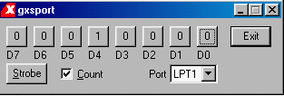
9. Suppose you would like to use the General Purpose Switches, SW6, SW7 and SW8 of the Digilab board to apply the inputs A, B and C, respectively. What pin numbers on the FPGA should you connect the inputs to?
10. To display the outputs S and Co on the LEDs 7 and 8, respectively, of the Digilab board, what pin numbers should you use of the signals S and Co?
11. The parallel port on the Digilab Board can be used for two purposes: (1) Programming the FPGA and (2) Parallel data communication. Which switch determines the mode of the parallel port. Give the switch number.
12. What is the power supply needed for the Spartan and the Spartan XL FPGA family of devices?
In-lab assignment:
A. Parts and Equipment:
Read the instructions carefully before doing the lab
You will enter the schematic and simulate the Sum and Carry-out function on the Xilinx Foundation Tools. This will be done by following the procedure explained in the tutorial webpages. Instead of doing the example in the tutorial you will be implementing the S and Co function in one schematic.
2. General Information (read this first before doing the assignment
explained in section 3 below).
You will implement the schematic diagram of the Sum and Co functions
shown in Figure 3. Follow the step by step
instructions in the tutorial. Save the schematic as "MYFA.SCH". The
inputs should be connected to an input pad (IPAD) with buffer and the output
pins should be connected to an output pad (OPAD) with buffer (see example
of Fig. 5 of
Schematic tutorial). It is a good practice to place the logic gates
first and connect them later. Try to be neat and organized when you draw
the schematic. You will be graded on the neatness of it. Also, it will
be much easier to read a schematic when it is clearly organized. Make sure
you name the input and output nets with the names A, B, C, Sum and Co,
respectively.
3. Start with the tutorial "Creating a new Project: Schematic Entry" on the Tutorial webpages. Instead of implementing the comparator circuit of Fig. 1 of the tutorial you will design the Full Adder of the pre-lab.
4. Proceed with the schematic entry as explained in the remainder of the tutorial (TOOLS -> DESIGN ENTRY -> SCHEMATIC ENTRY; or click on the Schematic Entry icon). It is a good idea to specify the page size before drawing the schematic otherwise the schematic may print too small. Go to FILE -> PAGE set up in the Schematic Editor window. Specify A size (8"x11").
- Launch the Xilinx Foundation Software by clicking on the Xilinx Foundation Project Manager Icon on the desktop.
- Open a new project and give it the name, MYFA (Don't give it the name of EasyProj). This project should be created in your folder (directory) that you just created: c:\users\your_name\). Use the Browse button to locate your directory (folder) on the C: drive.
- Under the flow, select Schematic.
- For Type, fill select F2.1i
- For family select from the pull-down menu "Spartan XL" (when using the Digilab board), XC4000E (when using the FPGA demoboard), XC5000XL (when using the XS40 board) or XS9500 (when using the XS95 board).
- For Part use S10XLPC84 (when using the Digilab Board), 4010EPC84 (FPGA demobaord - or name of the chip corresponding to the FPGA device on the FPGA demo board), 4005XLPC84 (XS40 board), or 95108PC84 (XS95 board). This refers to the target device you will later use to actually implement your design. You can change this at a later time.
- For speed, select grade 4 (can be changed later during the implementation process)
Start drawing the schematic. Add pin locations using the Symbol Properties window (Parameter Name: LOC and Parameter Description: P#) by double clicking on the pads. Choose the pin numbers according to the board you are using. Here are some sugggestions for the different boards:
When finished save the schematic. Put your name in the little table at the bottom right hand side of the sheet. This can be done by going to the FILE -> TABLE SETUP menu item (type in your and your partners name, Lab 2, Lab Title).
- Digilab board: connect the inputs to the general purpose switches SW1, SW2, SW3: e.g. A(P28), B(P27), and C(P26); connect the outputs to the LEDs, e.g. S(LD1 on pin P69) and Co(LD2 on pin P68).
- XS40 board: connect the inputs to the parallel port PC, e.g. A (P44), B(P45), C(P46); connect the output to a segment of the LED display, e.g. S (P19) and Co(P25). For a schematic drawing of the XS40 board and the position of the LEDs, click here.
- XS95 board: A (P46), B(P47), C(P48); connect the output to a segment of the LED display, e.g. S (P15) and Co(P21). For a schematic drawing of the XS95 board and the position of the LEDs, click here
- FPGA demoboard: connect the inputs to one of the general purpose switches SW3, e.g. A(P19), B(P20), C(P23); connect the output to one of the bar LEDs, e.g. S(P61) and Co(P62). For a schematic drawing of the demoboard and the position of the switches and LEDs, click here.
5. Next, you will do a functional simulation in order to check that the logic circuit gives you the required function (but no information yet about timing or delays; that will come later). Follow the tutorial on Functional Simulation for the Sum and Carry-out circuit.
Do now the Functional Simulation. Make sure that the "Functional" appears in the pull down menu at the bottom of the simulator window.
Check that your circuit works as expected and compare it with the truth table given in the pre-lab. Verify each entry. If the circuit does not work properly, check your schematic and correct it. Read also the section on "Common Mistakes". When you modify your schematic you should update the simulator. When the schematic has been modified save it and go to the OPTIONS menu -> EXPORT NETLIST and UPDATE SIMULATION in order to ensure that the simulator will use the latest schematic.
6. If the circuit works as expected write your name and date on the waveform (using the Graphics Tools by clicking on the bottom icon on the left side icon bar) and (select the bottom signal in the Waveform viewer and go to WAVEFORM -> COMMENTS window). Instead of printing the schematic and the waveforms, you will capture a screen of it and save it as a GIF file for insertion in your report. You can use the screen capture program (Hypersnap DX) that is installed on each PC. To find out how to use it, click on Hypersnap.
7. Implementation and testing
To download your design into the FPGA (or CPLD) and verify experimentally
that your circuit functions properly, you will first generate a configuration
file. This is done as follows:
Hand-in (at the start of next lab)
You have to hand in a short lab report that contains the following (see also Guidelines of Lab Report):