Digital Design Laboratory
Introduction to the Xilinx Foundation Tools
Introduction to the Xilinx Foundation System -
Schematic entry and Functional Simulation
Purpose:
The purpose of this lab is to get familiar with the Xilinx
Foundation Tools for designing, and simulating a logic circuit.
Pre-lab readings and assignment:
Before coming to the lab read the pre-lab section and answer all the
questions. Write the answers down in your lab notebook. See
guidelines
on keeping a notebook.
-
Background
You will be implementing a simple digital circuit, called a
half adder (HA). This circuit adds two bits together and gives a sum, S,
and carry, Co, output, shown below in the following examples.
A
1 1
+B +0
+1
---- ---- ----
C S
01 10
The first example adds 1+0, resulting in a sum S=1 and carry C=0. The second
example adds 1+1 resulting in a Carry=1 and a Sum=0. This can be accomplished
with a few logic gates, shown in the figure below.
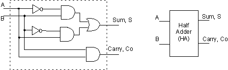
Figure 1: Schematic of a half adder circuit (HA)
This circuit consists of three AND gates, two inverters and one
OR gate. You can easily verify for yourself that this circuit performs
the desired function by applying an input to the gate and checking what
the output is. Do this for all four possible combinations of the input
signals A and B: AB=00, 01, 10 and 11 and fill out the table below.
Table for a half adder
| Inputs |
. |
. |
| A |
B |
Sum |
Co |
| 0 |
0 |
. |
. |
| 0 |
1 |
. |
. |
| 1 |
0 |
. |
. |
| 1 |
1 |
. |
. |
-
Reading:
-
Read the section on "Lab Safety"
-
Read the section on "Design
Flow Overview" , :Devices" and "Project Manager" of the tutorial "Getting
started with the Xilinx Foundation Tools".
-
Read the section on "Entering
a Schematic design"
-
Read the section on "Functional
Simulation"
- Pre-lab Questions (answers need to be submitted on Blackboard
before Tuesday noon, 1st day of the lab)
- Safety questions
- Questions about the Foundation Tools
In-lab assignment: F. Ketterer Lab, 204 Moore
A. Parts and Equipment:
1. PC with the Xilinx Foundation F2.1i software
B. Experiments
Read the instructions carefully before doing
the lab
You will enter the schematic and simulate the Sum and Carry-out function of
the Half Adder circuit using the Xilinx Foundation Tools. This will be done
by the procedure explained in the tutorial web pages.
While doing the experiments write down in your lab notebook what you did and
any observations and results. You can also sketch the schematics you implement
and note down the signal names. For an example of a notebook entry, click on
"Notebook
Entry Example"
1. First create a folder users\your_name on the C: drive in
which you will save your project. Give it your last name. Don't
use a name which is longer than 8 characters. Xilinx will cause
problems later on whenever you use names of folders and files which
have more than 8 characters. When you create a project in Xilinx, the program
creates a new folder with the same name as the project as well as a PDF
(project description) file, which it uses to recognize projects. Both
of these items should be placed in your folder.
2. Start with the tutorial "Creating
a new Project: Schematic Entry" on the Tutorial web pages.
-
Launch the Xilinx Foundation Software by clicking on the Xilinx Foundation
Project Manager Icon on the desktop.
-
Open a new project and give it the name, MYHA (Don't give it the
name of EasyProj). This project should be created in your folder (directory)
that you just created: c:\users\your_name\). Use the Browse button
to locate your directory (folder) on the C: drive.
-
Under the flow, select Schematic.
-
For Type, fill select F2.1i
-
For family select from the pull-down menu "Spartan XL" (when
using the Digilab board).
-
For Part use S10PC84. This refers to the target device you will
later use to actually implement your design. You can change this at a later
time.
-
For speed, select grade 4 (can be changed later during the implementation
process)
3. Proceed with the schematic entry of the half adder (Fig. 1) as explained
in the tutorial (TOOLS -> DESIGN ENTRY -> SCHEMATIC ENTRY; or click on
the Schematic Entry icon). It is a good idea to specify the page size before
drawing the schematic otherwise the schematic may print too small. Go to
FILE -> PAGE set up in the Schematic Editor window. Specify A size (8"x11").
Start drawing the schematic.
-
It is a good practice to place the logic gates first and connect them later.
Try to be neat and organized when you draw the schematic. You will be graded
on the neatness of it. Also, it will be much easier to read a schematic
when it is clearly organized.
-
Add I/O pins (termnals) for the two inputs A and B, and the outputs S and
Co, respectively. Give the terminals to proper direction (INPUT or OUTPUT).
When finished save the schematic. Put your name in the little table
at the bottom right hand side of the sheet. This can be done by going to
the FILE -> TABLE SETUP menu item (type in your and your partners name,
Lab 1, Lab Title).
4. Next, you will do a functional simulation in order
to check that the logic circuit gives you the required function. Follow
the tutorial on Functional
Simulation for the Sum and Carry signals.
Do the Functional Simulation. Make sure that the "Functional"
appears in the pull down menu at the bottom of the simulator window.
Check that your circuit works as expected and compare it with the
table given in the pre-lab. Verify each entry. If the circuit does not
work properly, check your schematic and correct it. Read also the section
on "Common Mistakes". When
you modify your schematic you should update the simulator. When the schematic
has been modified save it and go to the OPTIONS menu -> EXPORT NETLIST
and UPDATE SIMULATION in order to ensure that the simulator will
use the latest schematic.
5. If the circuit works as expected:
-
Write your name and date on the waveform (using the Graphics Tools by clicking
on the bottom icon on the left side icon bar) and (select the bottom
signal in the Waveform viewer and go to WAVEFORM -> COMMENTS window).
-
Instead of printing the schematic and the waveforms, you will capture a
screen of it and save it as a GIF file for insertion in your report. You
can use the screen capture program (Hypersnap DX) that is installed on
each PC. To find out how to use it, click on Hypersnap..
6. Saving or archiving your design: It will be a good idea to
save your project. Do not expect to find your project on the PC when you
come back! First archive your project: Select FILE -> ARCHIVE in the Project
Manager window and follow the Archive Project Wizard. This will generate
a MYHA.zip file in your folder. Next you can save your project either
on a ZIP disk or a floppy (if the file is not too large) or on your ENIAC
account (use FTP). In case you did not archive the project, you need to
transfer
both the .pdf file and the project folder
(in this case Myha.pdf AND Myha folder)!
If you have problems with any of the above tasks, see the instructor, TA
or one of the consultants during the scheduled lab times.
Hand-in (at the start of next lab)
You have to hand in a short lab report that contains the following (see
also Guidelines
of Lab Report):
-
Course Title, Lab no, Lab title, Session Name, Your name and date
-
Section on the Pre-lab showing the filled out table. Answers which were
submitted on-line do not have to be repeated here.
-
Section on the lab experiment:
-
Brief description of the lab experiment including the goals and discussion
on the theory of operation (if applicable).
-
Schematics of the circuit (insert the screen capture of your schematic
- make sure your name is on it)
-
Simulation waveform (use the screen shot of the timing waveforms)
-
Discussion of the results indicating that the circuit function properly.
You can for instance give a table and indicate that for each entry
the logic simulator give the right results for Sum and Carry.
-
Conclusion or discussion.
The lab report is an important part of the laboratory. Write it carefully,
be clear and well organized. It is the only way to convey that you did
a great job in the lab. It is preferred (but not necessary) that you type
the lab report. The report is due at the start of the next lab session.
Lab
notebook entry example
Back to EE201
Created by Jan Van der Spiegel; September
12, 1997; Updated by J. Van der Spiegel, September12, 2005.
Copyright, J. Van der Spiegel, 2004
 th visitor since 7/26/99