University of Pennsylvania
Department of Electrical
Engineering
Digital Design Laboratory
ESE201 Final Project
Electronic Dice Game
The
purpose of this lab is to:
- Design a digital circuit of an electronic dice game for two players.
- Learn to partition a digital system in a datapath and control unit
- Learn about timing issues between the control unit and datapath.
- Design a finite state machine for the control unit
- Design the datapath consisting of counters, registers, adders, multiplier and test logic
- Implement the circuit on a FPGA and verify its performance experimentally
Problem
statement and specifications
Your task is to design a digital circuit that emulates a dice game for two players. Each player has two dice that s/he throws simultaneously. The players roll the dice in sequence, one player after the other, until one of the players win. The game is played according to the following rules.
- Each player has 45 points at the start of a new game.
- Each player can place a bet equal to 0, 1, 2 or 3. The bet can be changed before one throws a new dice.
- When a player throws the dice and if the sum of the dice is 3, 8 or 10, the player receives a number of points equal to the sum of the dice multiplied by his/her bet, e.g. if the sum of the dice is “8” and his/her bet is 3 s/he receives 24 points. These points will be added to the previous amount s/he accumulated.
- However, if the sum is 4, 6 or 11, the player loses a number of points equal to the sum multiplied by his/her bet.
- If the sum is neither 3, 4, 6, 8, 10 nor 11, nothing happens and the next player has a chance to throw the dice.
- A player wins when s/he reaches a total of 90 points or more, or when the other player reaches 0 or less.
- When a player wins, one can start the game over again after pushing the reset button.
Since two dice are used, the sum will be between 2 and 12. The value of the dice can be generated by two independent counters who count between 1 and 6, or by a single counter who counts between 2 and 12. Each player has it own pushbutton (Roll Dice Rd1 and Rd2 for player 1 and 2, respectively) to roll the dice. The counter starts when a push button, Rd1 or Rd2 (Roll dice) is pressed and continues counting until the button is released. The clock used for the counter has a high frequency so that one cannot see the value of the counters when the push button is pressed. The number that the counter displays when the button is released is the value of the dice and will determine the outcome of the throw according to the rules given above.
In order to be able to follow the game, you will display the value of the dice and the total points accumulated on seven-segment displays. Since only 4 seven-segment displays are available on the Digilab board, you will display these values either for player 1 or player 2, depending on who is currently playing. An LED will light up when player 1 plays and another LED will go on for the other player. In addition, a “Win Player 1” or “Win Player 2” LED will go on when player 1 or player 2 wins, respectively.
The value of the bet will be entered using two general-purpose switches. A reset button brings the circuit into the initial state and loads the Points Registers with the initial value of “45”.
A demo of the electronic dice game is to be given to the lab instructors at the end of the second week of the lab.
Pre-lab
assignments
As with any complex digital system, the electronic dice game can be designed by using a modular and hierarchical design strategy. A common way to partition a system is into a datapath and a control unit. The datapath performs operations on the data and consists of registers (for storage, shift, counters), and combinational circuits (add, subtract, etc). The control unit determines the type of operation and the right sequence in which the datapath executes the operations. A schematic block diagram of such a partitioning is shown in Fig. 1 below. The control unit provides control signals to the datapath (such as Load, Shift, etc.) while the datapath provides the control unit with data inputs and status signals.
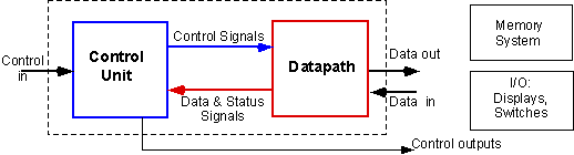
Figure 1: Partitioning of a digital system in a Datapath and Control Unit.
In addition to the control unit and datapath, a digital system further consists of memory and input/output units such as displays, etc. In the electronic dice game project you will not be using an external memory. However, output data will be shown on seven-segments displays and data will be inputted through switches and push buttons.
Datapath
A possible block diagram of the datapath of the electronic dice game is shown in Fig. 2.
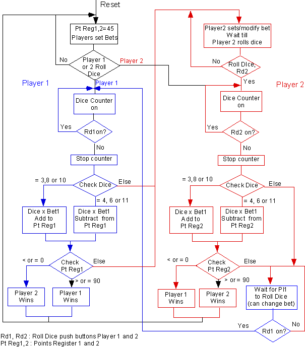
Figure 2: Datapath of the Electronic Dice Game
The datapath consists of a counter, registers, multiplexers and combinational circuits. The clock inputs at the registers and the counter are not shown. A 2-to-12 counter represents the sum of the dice and starts counting as soon as one of the Roll Dice push buttons has been pressed. The value of the dice (when the counter stops) is multiplied by the value of the bet of player 1 or 2, depending on which player is currently playing. The multiplied value is added or subtracted from the value stored in the point register. Negative values are presented in 2’s complement. Whether the value is added or subtracted depends on the results of the tests performed by the Test Logic. It is the control unit that generates the Add/Subtract signal. The Test Logic also checks the value of the point registers and provides input to the Control Unit, which determines whether a game is over or not, and which player wins.
Notice that the above block diagram is not the only way to realize the circuit. One can implement the dice game in various ways. For instance, you may want to use two 2-to-6 counters which are started by pressing two different buttons and then adding the two counts together. Instead of implementing the multiplier as a combinational circuit you can also implement it as a sequential circuit. You also may want to store the value of the bets into their own registers, etc. To a certain extent, it is up to you to decide how to realize the dice game.
Control Unit
The Control Unit initiates the game after it receives a signal from one of the Roll Dice push buttons. It goes through a sequence of states, depending on the status signals (TestA and TestB) from the Test Logic, which provides information about the value of the dice and the contents of the point registers. Based on the signals it generates, at the proper time, the control signals ST (Start counting or rolling the dice), LD1 (Load Register1), LD2 (Load Register2), and PL (player) determine the operation to be performed by the datapath.
Flow diagram of the Dice Game
In order to help you with the design of the state diagram of the control unit, it will be helpful to draw a flowchart of the dice game. The following figure shows a possible flowchart outlining the main steps and conditions during the game. Check this chart carefully. You can make some modifications to reflect your design approach. As with each design project there are no unique solutions. Notice that the flowchart of Fig. 3 is not an Algorithmic State Machine (ASM), although it can be used to derive a corresponding ASM.

Figure 3: Flowchart of the Dice Game
Question 1: (to be submitted on Blackboard)
The data lines in the datapath are indicated in blue and fat lines in the block diagram of Figure 2. These are busses carrying the signals. Give the width of each bus.
- What is the width of the point registers and the associated databus? (Hint: the register can have a value of up to 89+36=125 and as small as 1-36=-35; you need to be able to distinguish between positive and negative numbers). Negative numbers are expressed in 2’s complement.
b. What is the width of the bus at the output of the 2-to-12 counter and the output of the multiplier?
Question 2: (to be submitted on Blackboard)
a. Assume that the Points Register of Player1 has 73 points and that of Player2 has 77 points stored. Player 1 has made a bet of 2 while player 2 has a bet of 3. Player 1 is next and throws a 4, followed by Player2 who throws an 8. Give the contents of the Point Registers after each throw.
- After Player1 throws “4”: what is the value of Point Reg1 and Point Reg2 (in binary)?
- After Player2 throws “8”: give the contents of Point Reg1 and Point Reg2.
In case a number is negative, express it in 2’s complement.
b. Same question as above except the current value of the Point Registers is 89 and 17 for Reg1 and Reg2, respectively. Player1 rolls a “2” while Player2 throws an “11” (decimal). The bets are the same as in part a.
- After Player1 throws 2: what is the value of Point Reg1 and Point Reg2 (in binary)?
- After Player2 throws 11: give the contents of Point Reg1 and Point Reg2.
In case a number is negative, express it in 2’s complement.
Tasks:
Your task is to design each module and put these modules together in an overall system. In designing the modules you can choose from a variety of methods, such as schematic with gates, use predefined blocks or use a VHDL description.
Task 1: State Diagram of the Control Circuit.
Based on the understanding of the above flowchart, draw the state diagram of the control unit.
- Identify the input and output signals (see Fig. 2)
- Draw the state diagram. The outputs can be of the Mealy or Moore type. It is possible to mix both, as long as one does not change the type of a particular output. Remember that the Moore type outputs will change at the following clock edge after the input has changed. On the other hand, a Mealy type output can change as soon as the input is applied. Be aware of the timing differences.
- Identify on your state diagram the conditions of each transition, and the outputs associated with the transition (Mealy output) or with the state actions (Moore output). Keep the corresponding operations of the datapath in mind when you design your state diagram. Each output of your state diagram will generate an operation in the datapath. Follow the logical sequence of these operations while designing the state diagram
- Write the state diagram down in the lab notebook. Label each state, transition and output.
Task 2: Realization of the 2-to-12 counter.
Design a counter that counts in the sequence 2, 3, 4 . . .12, 2, etc. Since this counter counts only when one of the “Roll Dice” buttons is pressed, it should have a Count Enable (CE) input. Show the circuit schematic of such a counter. You can design this counter in a variety of ways. One way is to start from a state diagram that cycles through all 11 states. An alternative way is to use a 4-bit counter with parallel load with some external logic to accomplish the 2-to-12 count sequence. The Foundation Library has 4-bit counters with parallel load and Count Enable inputs available. All you need to do is to make it a 2-to-12 counter. Draw the circuit in your lab notebook.
Task 3: Realization of the Multiplier.
This circuit multiplies a 4-bit number with a 2-bit number. Since this is a relatively small multiplier, a combinational circuit may be a good choice. There are various ways to design such a multiplier. One way is to use the schematic discussed in class (See M. Mano and C. Kime, section 3-11, pp 144-145 – or in any textbook on Digital Design). An alternative way is to use a VHDL description of the multiplier, either a structural or behavioral (concurrent) description – see VHDL Tutorial).
Draw the circuit schematic or give the VHDL code of the multiplier in your lab notebook.
Task 4: Adder/Subtractor Circuit
Also here a variety of choices are available. You can use your previously designed adder circuit (or several of these) modified to make it an adder/subtractor. Alternatively you can write a VHDL code to perform this operation. Write your design choice in your lab notebook.
Task 5: Test Logic
This circuit performs two checks. One is on the sum of the dice. It generates control signals to indicate if the sum is 3, 8 or 10; or 4, 6 or 11; or neither of these values. The other test is performed on the values of the two point registers. It checks which register reaches first the value 90 (or above) or 0 (or below).
The easiest way to design this circuit is to write a VHDL code using the “Process” construct. Write the code for the test circuit in your lab notebook.
Task 6: Registers
The registers are used to store the points accumulated by each player. These registers should be registers with parallel load. At the start of the game, the registers are pre-set to the initial value of 45. You can build this register from D flip-flops (see e.g. Fig. 5-2 in Mano and Kime, or in similar textbooks on Digital Design). You just need to set or reset the individual flip-flops to the initial value of 45. An alternative way is to define the register in VHDL using the “Process” construct.
The Load signals will load the parallel inputs at the next clock cycle, as shown in the Fig. 4.
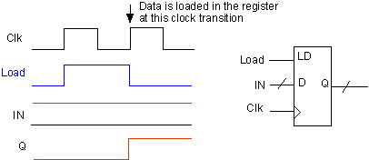
Figure 4: Timing of the Load signal for the Registers.
Task 7: Display unit
In order to be able to follow the operation of the game, you will display the value of the dice and the value of the accumulated points in the Points Registers. The value of the dice will be displayed on the first two seven-segment displays while the value of the Points Register will be shown on the last two seven-segment displays. Since only 4 seven-segment displays are available, you can also show these values for one player at a time. When player 1 or player 2 rolls the dice, you will show the dice and points for player 1 or player 2, respectively. This means that after the first player rolls the dice, the displays should show the value of his/her dice and value stored in the first player’s point register. Similarly after the 2nd player has rolled the dice. A LED will indicate whose values are being displayed.
This will require two decoders, one for the dice and one for the Points Register. These are similar to the decoders you have designed earlier for the 4-bit adder, except that the decoder for the Points Register has many more inputs.
In-lab assignments
A. Parts and Equipment:
1. PC
2. Xilinx Foundation Tools F2.1i
3. Digilab board, the Xilinx FPGA Demoboard (with XChecker cable and AC Adapter), XS40 or XS95 boards.
B.
Experiments:
Your goal is to design and implement the Electronic Dice Game on a FGPA. The lab is considerably more complex than the previous ones. It will be very important that you work systematically and give yourself enough time to design and debug the system. Debugging is a normal part of any design task.
You will partition the system in smaller modules. After you design each module, simulate it thoroughly and make sure that it works as expected. Do not skip this step since finding an error later on will be much more difficult. Once you have designed and simulated a module add it to the top circuit schematic and do a simulation of the partial schematic so that you make sure that the blocks work together. Simulating and testing your design progressively will make it easier to find errors. Errors may be the result not only of wrong circuit design but also due to timing or synchronization errors that may show up only when you link blocks together.
Open a new project, called MyDiceGm (8 characters only!) in the Schematic Flow mode. Place it in your folder in the user directory on the C: drive.
Task 1: Control Unit
- Design the sequential circuit for the Control Unit based on your pre-lab. The easiest way is to define it as a “State Diagram” using the State Editor. Since this module will be a macro, go to the TOOLS -> DESIGN WIZARD menu in the Schematic Editor or to TOOLS -> DESIGN ENTRY -> STATE EDITOR and create the ControlUnit macro. You can call this CntrUnit. You can use a combination of Mealy and Moore type outputs, as long as you use these consistently.
- When you finish with entering the State Diagram, check the syntax and synthesize the macro. Correct errors, if any.
- Simulate the control unit completely. Use keyboard strokes to simulate the input signals such as the Rolling of the dice, and the results of the Test Logic. Pay attention to the timing of the signals, in particular the load signals LD1, LD2 for the Point Registers to make sure it loads the proper values.
- Add the Control Unit macro to the top level schematic (if not done already).
Task 2: 2-to-12 Counter
- Create a macro for the counter that counts from 2 to 12 and back. Use your pre-lab design. The counter should have an Enable Count input.
- Add the counter to the top level schematic.
- Simulate the counter
Task 3: Combinational circuits: Multiplier, Adder/Subtractor, and Test Logic
- Create a macro of the 4x2 multiplier using your pre-lab design. You can use gates to define this multiplier or use a VHDL description. The latter is the simplest way to define the cell.
- When done, simulate the macro. If it works properly, save the simulated waveform and take a screen capture for use in your lab report.
- At the top level schematic, connect the multiplier to the output of the counter and simulate the counter-multiplier together and verify it works properly
- Do the same for each of the other circuits. Make sure you simulate each macro separately and together with the other macros.
Task 4: Point Registers
- Create a macro of the Point Registers. Each register needs to be set initially to “45” and have parallel load capabilities.
- Simulate the macro. If it works properly, save the simulated waveform and take a screen capture for use in your lab report.
- Add the macro to the top level schematic
Task 5: Complete the top level schematic
- Complete the top level schematic and interconnect the modules properly. Add the on-chip clock oscillator (OSC4) and use the F16K output. Add input and output buffers and pads. Label the pads
- Simulate the overall schematic including the Control Unit. Verify that the circuit works properly. Pay attention to the timing. Make sure that the right value is loaded into the registers. Take a screen capture of the waveform for use in your report.
- If problems occur find the error. If each module worked properly separately, but the overall circuit gives errors, there is a good chance that the error is the result of wrong timing. It is important that the control signals supplied by the control unit arrive at the right time (e.g. the Add/Subtract signal, Load signals for the Point Registers, etc.). Check if your control outputs generated by the Control Unit have a combinational or registered outputs, are Mealy or Moore type outputs. The timing of the signals will be different depending on the type of output you specified for it in the state diagram.
Task 6: Decoders and Switch circuit for the seven-segment displays
- Design the decoders for the value of the Dice and the value of the Point Registers
- Design the switching circuit needed to use the 4 seven-segment displays.
- Simulate the circuits
- Add the decoders and the switching circuit to the top level schematic
- Add input and output buffers and pads for the displays.
Task 7: Implementation, downloading and testing
- Implement the circuit. Check the type of FPGA you have on the board and make sure that the right FPGA is specified in the Project. If not, go to the FILE -> PROJECT TYPE menu in the Project Manager, and select the right FPGA family (e.g. Spartan, or SpartanXL) and chip (e.g. S10XLPC84).
- When the implementation has been successful, you need to define the pin numbers. This can be done with the Constraint Editor or by placing the pin number directly on the Pads, using the Pin Attributes. Use the following pins:
- Roll Dice: use the push buttons BTN1 and BTN2
- Reset: use push button BTN4
- For the bets use the general-purpose switches: Player 1: use SW1 and SW2, and for Player 2 use SW3 and SW4.
- To indicate which player is the player use the LEDS; Player 1: LD1, Player 2: LD2.
- For the Win1 and Win2 lights, use LED LD7 and LD8.
- Define also the pins for the cathodes and anodes of the seven-segment displays.
- If you used the Constraint Editor to define the pin locations, you need to invoke the interactive flow engine to implement the circuit using the updated constraint file. Check the Pad report after you run the implementation and verify that the pads have been assigned to the right pin numbers. In case you have difficulties assigning the right pin numbers with the Constraint Editor, edit the user constraint file directly using the VHDL editor.
- Download the file into the FPGA.
- Test the Electronic Dice Game:
- Reset the circuit and verify that the number 45 is displayed for the Point Register.
- Each player sets a bet (1, 2 or 3) using the general-purpose switches.
- Start the game: Player 1 pushes the Roll Dice button. Check the value of the dice and the new value of the Point Register. Check if the value corresponds to the rules of the game. Next, Player 2 pushes the Roll Dice button. Check the result. Keep playing until one of the players win. Enjoy the game.
- If the circuit does not work properly go back and try to identify what goes wrong. Check the pad report to make sure the right pins have been assigned. Go back to the schematic, debug and modify the circuit, re-simulate and implement the new design. It is not unusual that the circuit does not work on the first try. Debugging is an integral part of the learning process. Try to trace the error back based on the results obtained during the testing. Check that the simulations work according to Specs.
Task 8: Give a demo to the Lab Instructor
Play the game with the lab instructor and convince him/her that it works according to the rules specified for the game. No bribes allowed!
Hand
in:
You must hand in a lab report that contains the following:
1. Course Title, Lab no, Lab title, your name and date.
2. Section on the Pre-lab with answers to all questions (only those task that were not submitted online) [15pts].
3. Section on the lab experiment:
a. Brief description of the lab experiment including the goals.
b. Copy of the schematics (screen capture) and HDL source code of each macro (screen capture)
c. Simulation results with Screen capture of the major macros
d. Summary of the Device utilization.
e. Discussion of the results indicating that the circuit functions properly.
4. Conclusion.
The lab report is an important part of the laboratory. Write it carefully, be clear and well organized. It is the only way to convey that you did a great job in the lab.
References
- M. Mano and C. Kime, "Logic and Computer Design Fundamentals," 2nd Edition, Prentice Hall, Upper Saddle River, NJ, 2001.
- C. Roth: “Fundamentals of Logic Design,” 4th edition, PWS Publishing Company, New York, 2000.
- R. Katz, "Contemporary Logic Design", Benjamin/Cummings Publishers, Reading, MA, 1994.
- J. F. Wakerly, "Digital Design," 3rd edition, Prentice Hall, Upper Saddle River, NJ, 2000.
- P. Horowitz and W. Hill, "The Art of Electronics", Cambridge University Press, Cambridge, 1989; p506.
©2001, Jan Van der Spiegel; Created November 15, 2001; updated December 11, 2001