![]()
작성일: 2005.09.19
![]()
FPGA Clock
Schemes
By
Tim Behne, Embedded Systems Programming
March 13, 2003 (8:30 p.m.
EST)
URL: http://www.eetimes.com/story/OEG20030210S0053 또는 http://www.us.design-reuse.com/news/?id=4854
One of the most important steps in the design process is to identify how many different clocks to use and how to route them. This article tells you how to use routing resources efficiently.
Field-programmable gate arrays (FPGAs) have long had a prominent position in the world of signal processing and embedded systems. By implementing calculations in hardware, they can process data at rates much higher than the fastest microprocessors. The increasing flexibility and affordability of FPGAs have also made them attractive alternatives to application-specific integrated circuits (ASICs), particularly in small-to-medium volume applications.
As larger designs are implemented in FPGAs, it is likely that many of them will have multiple data paths running on multiple clocks. An FPGA design that contains multiple clocks requires special attention. Issues to focus on are maximum clock rates and skew, maximum number of clocks, asynchronous clock design, and clock/data relationships.
Time
bandits
The first step in any FPGA design is to decide what
clock speed is needed within the FPGA. The fastest clock in the design
will determine the clock rate that the FPGA must be able to handle. The
maximum clock rate is determined by the propagation time, P, of a signal
between two flip-flops in the design. If P is greater than the clock
period, T, then when the signal changes at one flip-flop, it doesn't
change at the next stage of logic until two clock cycles later. Figure 1
shows this.
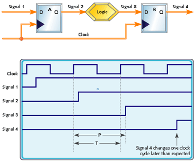
Figure 1: An undesirable propagation effect
The propagation time is the sum of the hold time required for the signal to change at the output of th e first flip-flop, plus the delay of any combinatorial logic between stages, plus the routing delay between stages, plus the set-up time for the signal going into the flip-flop at the second stage. Later in this article, we will look at methods to increase the maximum clock rate supported by a design.
Each clock used in an FPGA design, no matter the rate of the clock, must have low skew. The skew, S, is the maximum delay from the clock input of one flip-flop to the clock input of another flip-flop. For the circuit to work properly, the skew must be less than the propagation time between the two flip-flops.
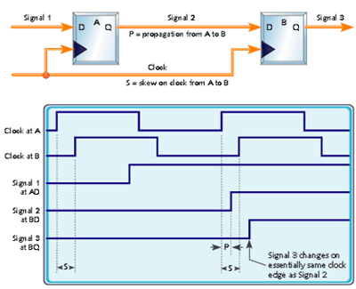
Figure 2: An undesirable skew effect
Figure 2 shows what will happen if the skew is greater than the propagation time (S > P). The intent of the circuit is to delay Signal 1 by two rising edges of the clock. However, a change in Signal 1 could propagate th rough to Signal 3 on the same clock cycle that caused the change at Signal 2. Because S > P, the circuit behaves incorrectly.
Notice that the clock rate does not play into this at all. Even a seemingly innocuous 100 bit/s clock can exhibit skew problems. This means that while FPGA vendors release chips with lower propagation times and higher clock rates, skew problems could potentially get worse, even in designs that do not run at anywhere near the maximum clock rate.
Fortunately, FPGA vendors are well aware of the problems caused by clock skew and offer low-skew routing resources within their chips. These are special routes that offer a guaranteed maximum skew between any two flip-flops within a certain domain inside the chip. Some of these low-skew resources cover the entire chip, while others might only cover a particular row or column of logic blocks within the FPGA. For a design that requires many different clock sources, these low-skew routing resources can become precious commodities.
One of the most serious problems associated with multiple clock designs is when two stages of logic are combined using asynchronous clocks. Asynchronous logic can create metastable states that can seriously degrade the performance of the design or completely destroy the functionality. A metastable state is created when the flip-flop's timing requirements (setup and hold times) are violated. The resulting output of the flip-flop is unknown, and can make the entire design nondeterministic. If one stage of logic asynchronously feeds data to another, it is difficult, if not impossible to meet the set-up and hold-time requirements of the flip-flop, as shown in Figure 3.
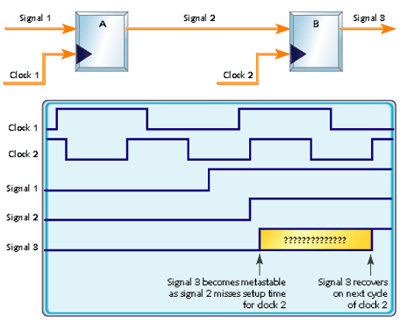
Figure 3: Metastability
To clarify, if the design contains asynchronous logic, metastability is likely to occur. Care must be taken when dealing with with asynchronous sources as they can be some of the most difficult problems to find once they make their way into a system.
Multiclock
designs
For the remainder of this discussion, let's consider
an E3 mux/demux design commonly used in the telecommunications industry.
Figure 4 shows the design. The multiplexer receives 16 independent E1
channels, each running at 2.048MHz, from a set of independent line
interface chips. These E1 streams are then combined into four E2 streams,
each running at 8.448MHz. The E2 streams are then combined into an E3
stream that's transmitted serially at a rate of 34.368Mbps.
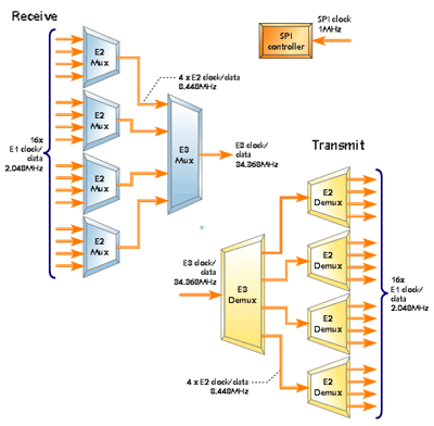
Figure 4: E3 multiplexer/demultiplexer
At the receiving end, the demultiplexer performs the inverse operation by extracting the four E2 data streams from the E3 stream and then the 16 E1 streams from the E2 streams. Finally, the E1 streams are transmitte d to the receiving line interface chips.
The E1 line interfaces operate independently for both transmit and receive. As a result, the corresponding 2.048MHz clocks could be running at slightly different rates (+/- 20ppm). Also, since most systems transmit and receive data simultaneously, the separate multiplexer and demultiplexer will be accommodating two independent E3 streams (transmit and receive). Consequently, both of the 34.368MHz clocks could be running at slightly different rates.
Since the E2 streams are created on-chip, the E2 muxes may all share the same 8.448MHz clock. However, since the received data rate is independent of the board we are designing (and we cannot assume we are getting data from a source that uses the same clock for all of the E2 muxes), the E2 demux clocks must be allowed to operate at slightly different rates.
Furthermore, let's assume that we have a separate serial peripheral interface (SPI) bus interface for status and control via a processor that operates with a 1MHz clock.
In all, we'll have thirty-two 2.048MHz clocks, five 8.448MHz clocks, two 34.368MHz clocks, and one 1MHz clock for a grand total of 40 clocks in the design. Clearly, this design will serve as an excellent test case for some of the issues that are covered in the remainder of this article.
The fastest clock in our example design is the 34.368MHz E3 clock, which determines the minimum speed rating of the FPGA. The maximum clock rate for an FPGA is not trivial to determine, since differences in designs will affect the maximum. However, you can usually find parameters called "Global Clock Setup and Hold Time" and "Clock to CLB Outputs." Summing the two largest values found in the data sheet and adding 25% will result in roughly the minimum allowable clock period. It is good practice to allow for at least a 10% overhead on the maximum clock rate to guarantee operation over temperature. Therefore, in our example, we set our minimum allowable speed rating to 40MHz. Most newer FPGAs can easily support this frequency. In fact, FPGA vendors are advertising rates in excess of 300MHz.
Once you have settled on an FPGA that meets our maximum frequency requirement, you must ensure that the device has enough room to fit your design comfortably. If the FPGA is almost full, there may not be enough routing resources available to meet the timing constraints of the design. Be advised that the advertised rate is the best-case scenario rate. FPGA vendors typically suggest that the FPGA logic can go to about 80% full before the routing performance starts to degrade noticeably. Choosing to err on the side of caution, I recommend starting most new designs with the FPGA logic about 50% full. This allows slop for any errors made in calculating the initial design size and gives room for the inevitable "feature creep" that occurs after a design is started. If the final design occupies less than 50% of the FPGA's real estate, you can then achieve a cost reduction by going with a smaller FPGA in the same family.
The routing of the fastest clock in the design can be improved by specifying the rates on the slower clocks via timing constraints. In our multiplexer example, if you tell the FPGA routing tool that the SPI bus clock is 1MHz while the E3 clock is 40MHz, then it will attempt to lay the circuit out such that all the logic blocks that use the E3 clock are close together. If any circuits need to be spread out due to space limitations, it will first spread out the SPI logic since that can handle longer propagation delays. All FPGA vendor routing tools have methods for specifying these slower clock rates.
Local or
global
As mentioned previously, all FPGAs have special
low-skew resources for routing clocks. Some devices have dedicated clock
inputs that feed directly to the low-skew resources, while others have
low-skew buffers inside the FPGA that can be sourced from anywhere. Some
clock resources are global and can feed logic to any part of the device.
Other resources are local and can only distribute a clock in a certain
area of the device. It is important to make sure that clocks that drive
many gates are on global nets. A clock that drives only a small amount of
logic, like the SPI clock in our example, can go on a local net.
Despite its importance in choosing the right device, it is not always easy to tell how many clock resources are on a particular chip by a perfunctory examination of its data sheet. Clock resource information is usually found under "Clock Distribution" or "Global Clock Buffers" on FPGA data sheets. The Xilinx Spartan II 100, for example, has four global clock resources and 24 local resources. The Altera APEX 20K 100 contains eight global clock resources and no local resources. The newer Xilinx Virtex II 70 contains 16 global clocks and no locals, while by comparison the Altera APEX II 70 contains eight global clocks and no locals. Some special resources such as DLLs (Dynamic Link Libraries-a Xilink term), PLLs (phas e-locked loop-an Altera term), and clock multipliers use up some of the low-skew resources, so remember to keep this in mind if you need to use these types of functions.
Upon inspection of the FPGA market, it appears there is no device with adequate clock resources to support the 40 clocks needed for our mux/demux design. So we'll need to use some tricks to reduce the number of clocks used in our design.
Reducing
clocks
Let's begin by looking at the clocks for the E2 and
E3 multiplexers. We have already stated the acceptability of running all
four E2 multiplexers with the same clock; the E3 multiplexer, running at a
much higher rate, must have a different clock. However, what if we derive
the E2 clocks from the E3 clock? Since we know when the E3 multiplexer
wants data from each of the E2 tributaries, we can simply send clock
pulses to each E2 multiplexer when we want it to give us data. We have not
yet eliminated any clocks, but th e E2 clocks are now based on the E3
clock.
What if we also use the same clock on all the multiplexers and just use an enable signal to tell the E2 multiplexers when to operate? If the E3 mux creates the enable signals from its 34.368MHz clock, skew on these enable signals is not any more of a problem than it is for any other synchronous logic in the FPGA. Therefore, the enable signals can use normal (high-skew) routing, and we have just eliminated the need for the separate 8.448MHz multiplexer clock! The same concept can be used for reading the data out of the E1 data buffers. In other words, if the E2 multiplexer requires data, it can activate the enable signal to that particular buffer. The clock to the buffer itself can retain the 34.368MHz clock used by the E3 multiplexer, as seen in Figure 5.
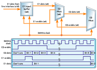
Figure 5: E3 MUX clock usage
Finally we examine the 16 E1 clocks ente ring the FPGA from the line interface chips. These clocks present several problems. First, 16 clocks would consume too much of the available clock routing resources. Second, with 16 asynchronous clocks driving flip-flops (in close proximity) within the same FPGA, one may experience noise problems due to ground bounce, crosstalk, and other effects. For example, a positive edge flip-flop can change state on the falling edge due to double clocking caused by noise. Such a problem is very difficult to isolate.
As a possible solution, we recommend using one fast clock to sample the 16 E1 clocks. To clarify, we know that each of the 16 input clocks will be close to 2.048MHz, and we have a 34.368MHz system clock. We can therefore sample each of the 16 E1 clocks with the 34.368MHz clock and store the results into a 16-bit register (one bit per E1 clock). Then we can employ an algorithm to detect low-to-high transitions on the E1 clocks, create an enable signal for each of the E1 data signals, and register the da ta (with the 34.368MHz clock) on the next cycle.
In order to be successful, there must be prior knowledge of the clock-data relationship to ensure that we do not sample data during a time that it may be changing, as illustrated in Figure 6. Note that two flip-flops are used in the first stage on the clock sampling circuit in order to tolerate metastability (more on this later). Also note that the data must be delayed by the same number of clock cycles as the clock.
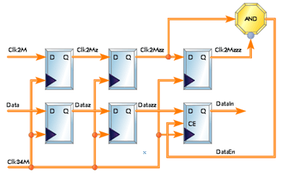
Figure 6: Clock oversampling in the
multiplexer
We have successfully reduced the mux-side to merely one clock. Can something similar be done on the demux side? The input clock for the E3 demultiplexer must be an external input. This is because the same off-chip device that drives the E3 input data sources this clock. Since the E3 demultiplexer knows when it is sending data to the E2 demultiplexers, it ca n create enable signals for each one, and the four E2 demultiplexers can all run on the same master clock as the E3 multiplexer. Likewise, the E2 multiplexers can create enable signals for the individual E1 streams.
If we assume that the line interface chip can accept gapped clocks (many of them can), we need only send a clock pulse to the line interface whenever the E1 enable signal is asserted. However, it is simpler just to send the enable signal itself to the interface chip without worrying about creating a new clock. Since the data sent to the interface will change on the falling edge of the enable signal (refer to Figure 5), we need to make sure that the interface will sample on the rising edge of the clock. Since the enable signal is used as a clock only at the line interface chip and not within the FPGA, there is no need to route it on a low-skew resource. Note that this only works when you know you will never have a case where you will want to send data to the same tributary on successive pulse s of the master clock.
The 1MHz SPI clock cannot be easily eliminated, but we have now reduced our original requirement of 40 clocks to just three by using enable signals and clock oversampling techniques. We can now implement our design on a much wider range of devices.
Asynchronicity
Before creating any logic with
asynchronous clocking, you should exhaustively consider another
alternative. Combining logic stages with asynchronous clocks is a dominant
source of problems. Again, when a flip-flop's setup and hold time
constraints are violated, the output becomes unpredictable for a short
amount of time and will eventually settle to a "1" or "0". Which state it
will settle in is impossible to predict.
In the July and August 2001 issues of Embedded Systems Programming, Jack Ganssle wrote a pair of columns on asynchronicity and metastability that should b e required reading for any logic designer. Please refer to those articles for an in-depth look at metastability.
Fortunately, there are some solutions to the problems of metastability. The solution illustrated in Figure 6 is the double-registering technique. Data coming into the first flip-flop is asynchronous with the clock, so the first flip-flop will almost certainly go metastable. However, the second flip-flop will never go metastable as long as the length of metastability is less than the period of the clock. (Unfortunately, FPGA vendors rarely publish metastability times, though they are typically less than the sum of the set-up and hold time of the flip-flop.)
If the clock is not too fast to meet normal timing constraints, it is probably not going to propagate metastable states in a circuit such as Figure 6. Even though the output of the first flip-flop can be used as long as all of the paths out go to flip-flops clocked by the same clock, it is generally good practice to use a circuit such a s that in Figure 6 to isolate metastability to one short line. That way, it is less likely that a future change to the circuit will unintentionally use the metastable line in nonclocked logic.
If the data being read is a counter, such as read or write addresses from an asynchronous FIFO, you should consider the following caveat. A traditional 3-bit counter can have one, two, or three bits changing between states. For example, if the read occurs at the instance when the counter is changing from "011" to "100," then the state of all three bits is unknown, and the read value can be any of the eight possible states.
Table 1: A 3-bit grey
code
000
001
011
010
110
111
101
100
If the counter is built using a grey code, such as in Table 1, then only one bit can change from one state to the next. If the read occurs at the instance that the counter is changing, then only one bit will be in question, and there are o nly two possible outcomes to the read operation. Furthermore, the two possible values will be the value of the counter just before the read and the value of the counter just after the read. Since the read occurred at a time when the counter was in transition, it is impossible to say with certainty that one value is correct while the other is not. In other words, either value should be considered valid.
Another way to avoid problems with asynchronous clocks is to ignore the slower clock and sample the data with the faster clock (if you know which one is faster). This requires that the data have special framing characters (a preamble, for example) to define the data boundary. This is a common practice and can be found in nearly every embedded system in the form of a UART. A very fast clock, say 16 times the data symbol rate, will sample until 15 consecutive start characters are found. The design then declares that the next 16 (or so) bits correspond to the first bit sent, the next 16 (or so) bits are the n ext bit, and so on.
Countdown
As
FPGAs increase in density and become more affordable, the number of
embedded products that we see using FPGAs will continue to grow rapidly.
As these designs get more complex, a lot of design issues stemming from
multiple clocks are sure to arise. Paying special consideration to the
maximum clock rate, the number of clocks, and asynchronous clocks in the
initial design phase can alleviate many problems. These same factors can
then be used to pick an FPGA that suits all the needs of the design. esp
Tim Behne has worked in embedded systems for nearly a decade. He has a BSEE from Texas A&M University and an MSCE from the University of Houston--Clear Lake. Tim is currently the manager of software and signal processing at Microwave Networks. You may contact him at timothyb@microwavenetworks.com.
Note
Tim would like to thank Tom Cassaro for his contributions to this article.
Copyright © 2003 CMP Media, LLC | Privacy Statement
![]()
![]() Send to a colleague |
Send to a colleague | ![]() Print this document
Print this document