![]()
|
|
![]()
An FPGA primer for ASIC designers
By Rafey Mahmud, EEdesign.com
Apr 15, 2004 (6:00 PM EDT)
URL: http://www.eedesign.com/article/showArticle.jhtml?articleId=18901725
With the advent of new technologies in IC design and complexity of the business models, chip designers may want to explore different choices available to them for implementation. ASICs have been the most natural choice for those who want the highest performance at a low unit cost. But with mask costs approaching a one million dollar price tag, and NRE costs in the neighborhood of another million dollars, it is very difficult to justify an ASIC for low unit volumes.
FPGAs, on the other hand, have improved their capacity to build systems on a chip, with more than one hundred thousand logic elements and tens of millions of bits of on-chip RAM available. However, the unit cost for FPGAs is still pretty high. Meanwhile, structured ASICs combine the cost advantage of ASICs with the low-risk solution of an FPGA.
FPGAs offer a low risk, quick time to market solution. There are no significant NRE costs associated with an FPGA design. Structured ASICs, on the other hand, try to cater to mid-volume products. They offer all the advantages of an FPGA design but the low unit cost of an ASIC for mid-volume production.
Cost is one consideration only. There are many other technical factors that affect the time to market of a design. FPGAs, for example, have a very integrated environment where I/O buffers, boundary scan, clock trees, and PLLs are pre-included in the design environment. The timing constraints are specified based on very accurate modeling of the final system, requiring fewer iterations to meet the final timing goals.
With technological innovations and shrinking device geometries, FPGAs have evolved as formidable competitors to ASICs for implementing systems on chips. While the FPGA design flow has many similarities to a typical ASIC design flow, it requires a different mindset from ASIC design.
Counting gates
ASIC designers are used to defining their chip size in terms of number of gates. This concept, if applied to FPGAs, can be very misleading. For estimating ASIC density, the total area of the chip is divided by the area of a two-input NAND gate to derive the number of gates. Usually, memories are included in the area calculation.
When a chip architect is trying to determine if their design will fit in a given FPGA, trying to figure out how many equivalent gates an FPGA family has is virtually impossible and misleading. FPGA data sheets will give you total number of logic elements and size of the memories in a device. Logic elements cannot be equated to ASIC gates, because depending on the synthesis tool, the same logic element can be used in many different ways, performing the task of several ASIC gates.
The size estimate of an FPGA comes from targeting the design into a device to see how well it fits. Timing wise, as a general rule of thumb, standard cell ASICs in a similar technology are two to three times faster than their FPGA counterparts due to configurable routing in FPGAs.
Of course, the maximum frequency a chip can run at depends a lot on the design characteristics, and cannot be accurately predicted. For example, DSPs and memories are highly optimized and pre-defused in a typical FPGA and are thus comparable to ASIC DSP or memory in terms of size and performance.
I/O pads in an FPGA are pre-inserted, with most popular I/O standards included. Designers should ensure that all the standards needed by their design are present in the device they pick.
How ASIC and FPGA flows differ
There are many steps in the ASIC design flow methodology which are not needed for an FPGA based design. Design for testability, including memory BIST, is not needed. Clock tree generation, signal integrity checks, and design rule checks are not needed. Most physical verification steps are not needed.
The biggest advantage of an FPGA implementation is the ease and speed of functional verification. RTL simulations can be performed just like for ASICs, but being able to configure an actual device and running real-time stimulus in the lab gives a great advantage in the verification effort.
When a design is targeted to an FPGA device, the timing analysis results and fitting results you get are absolutely complete. In ASICs, designers are used to getting piecemeal results as separate steps of I/O insertion, boundary scan insertion, test circuitry insertion and block integration are performed. In FPGAs, due to a highly integrated environment, everything needed for the design is there; thus the timing results are complete from the beginning.
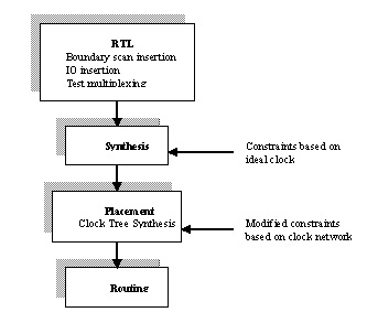
Figure 1 - A
typical ASIC flow
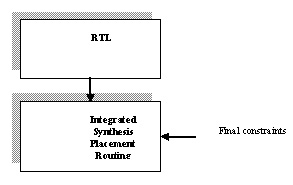
Figure 2 - A
typical FPGA flow
As you can see by comparing figure 1 with figure 2, manual work that is often required to insert I/O buffers, boundary scan and test-related multiplexing at the top level of an ASIC's RTL code is not needed for an FPGA design flow. Furthermore, due to a highly integrated synthesis, placement and routing flow, not many design iterations are needed.
For example, in a typical ASIC design flow, chip-level I/O timing constraints are first specified with respect to an ideal clock. When the clock trees are synthesized after placement, the timing constraints need to be readjusted to the actual insertion delay of the clock network. In FPGAs the clock trees are pre-synthesized, so all the constraints are final. All FPGAs have PLLs which can then be used to phase shift the clock to help meet changing I/O timing requirements.
ASIC standard cell libraries have many variations of gates, with different drive strengths and input widths. Furthermore, routing is decided based on placement and buffers can be inserted as needed to meet goals of the design.
In FPGAs, configurable routing eats up most of the timing budget. Therefore it is advisable for logic designers to code RTL in a way that avoids use of wide-input gates and high fan-out nets. It is therefore better to have more parallel state machines with less total number of states, rather than one state machine with a large number of states.
In an ASIC design, using a smaller number of flip-flops in a design means saving power consumption and area, but in FPGAs the registers are already there, and not using some of them would not save any area or power consumption.
From a system-on-chip perspective, FPGAs have embedded memories that are limited in total amount, but different configurations are available. For example, you can either use three 8M memories or one 24M memory configuration.
DSPs are highly optimized and RTL can be written in a way that synthesis tools can map it to the right DSP automatically. There are system builder tools available to automatically integrate different components of a system, like processors and peripherals, and generate RTL for in-between busses. There are soft and hard cores available for different standard and proprietary processors.
Clock considerations
ASIC designers use gated clocks to selectively shut down clock networks to save dynamic power consumption. ASIC layout tools can easily balance the clock network delay of gated-clocks with non-gated clocks, but such is not the case in FPGAs, as clock trees are pre-synthesized.
Adding a gate in one clock network domain often skews it with respect to another clock network domain, causing hold time violations. Two approaches are advisable for designers when trying to implement gated clocks:
1. Try to treat cross clock-domain paths as asynchronous paths by implementing the right protocol and synchronizers, such that cross-clock domain paths don't need to meet setup and hold requirements.
2. Use PLL enable control pins for shutting the output of the PLL off under application control, instead of using gated clocks.
Working with PLLs
Most FPGA suppliers include phase-locked loop circuits on their chips. PLLs enable low frequency clocks fed to the chip from the outside world to be multiplied in frequency for internal operations. In addition to multiplying and dividing frequency of a clock, PLLs with on-chip feedback paths help distribute the clock signal through out the chip with less dependence on process and temperature variations.
As shown in figure 3, a programmable PLL can be used to shift the phase of an internal clock to adjust the total insertion delay of the clock network in an FPGA. Programmable phase shift helps the chip accommodate for unexpected deviations in data delays on the board. The software timing analysis tools always include timing models of PLLs during compile.
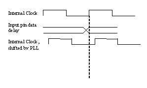
Figure 3 -
Programmable PLL helps meet I/O constraints
The synchronous versus asynchronous reset methodology approach in FPGAs is a little different than ASICs. In FPGAs, synchronous and asynchronous reset circuitry is already built into each flip flop, so you cannot save any area by using one versus the other.
There are many advantages and limitations of an FPGA based design, but the designers have to approach the FPGAs with a different mindset. Making informed choices from the architecture to the RTL phase can help you meet your goals by taking advantage of FPGAs.
Rafey Mahmud is a member of technical staff at Altera Corp. He has worked on several microprocessor and ASIC design projects.
Copyright © 2003 CMP Media, LLC | Privacy Statement
![]()
|
|
|
|