![]()
|
|
|
|
 |

Corralled - Get hold of wire delays
The physical and dynamic characteristics of wires on a die dictate the topology of an IC. Soon, they will dictate its entire architecture.
SVP (silicon virtual proto-typing) is a creature of the new millennium. Until three years ago, gate delays represented the most significant portion of a signal-propagation time. Therefore, engineers could approximate interconnect delay well enough and could design circuits without paying much attention to place-ment-and-routing issues. A logic designer needed to know little about chip layout, and layout engineers need not have worried about logic design. Logic synthesis automatically adjusted the strength of signal drivers to meet propagation-delay requirements, and designers did not need to worry about the physical characteristics of the conductor carrying the signal. Even the most challenging designs required little knowledge of electronics or physics: Boolean logic was enough.
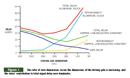
Things changed with the advent of 180nm processes: Wire delays became more relevant than gate delays. Gates are now smaller than most of the interconnecting wires, so propagation delays in the wire are significantly greater than gate delays. In addition, the calculation of the delay that wiring causes must take into account second- and third-order parameters. For example, crosstalk depends not only on the physical characteristics of the wire, but also on the placement and behavior of neighboring wires. You cannot, therefore, obtain a satisfactory estimate of wire delay without knowing something about the topology of the final product. Designers are finding that circuits that must operate at high frequency or with low power are the most susceptible to crosstalk, even on a pc board. The reason for this phenomenon is that, especially in IC design, the ratio of wire dimensions versus the dimensions of the driving gate is increasing, and the wires' contribution to total signal delay now dominates (Figure 1).
The Problem
A number of factors contribute to the propagation-delay and power-consumption values. Signal integrity results from the dynamic environment surrounding an active wire. As long as wire-propagation delay represented a small portion of the total propagation delay, designers could use a nominal value and evaluate the circuit performance using static-timing analysis. Designs at 180 and 130nm require precise values for the interconnecting wire and its place on the die in relation to neighboring wires to enable designers to accurately predict the behavior of the circuit. Engineers designing for 90nm processes will likely have to use dynamic-timing analysis to predict circuit behavior. The strength of the signal the circuit carries and the location of adjoining wires will be insufficient to determine the circuit's function. Whether any of the adjoining wires are simultaneously active and the strength of the signals that are active concurrently will also factor in the results.
Designers must worry about a number of physical attributes of the circuit they are developing. Resistance in the power-and ground-distribution grid causes IR drop. Power- and ground-wire resistivity increases with decreasing geometries, while designers continue to try to decrease the overall power-supply voltage, especially in portable devices. Gate delays increase nonlinearly as voltage at gates decreases. The result is poor performance and increased susceptibility to noise. It is therefore imperative to understand how to distribute power to the system and the impact that the topology of the power circuit has on the physical behavior of the logic circuit. Coupling-capacitance and inductance effects increase with decreasing size of the process geometries. When a signal-state transition occurs in neighboring wires, the coupling capacitance between the wires can cause crosstalk. The amount of crosstalk depends on the capacitance between wires and the switching speed of the signals. Crosstalk causes signal degradation when a transition on an aggressor wire causes a glitch to appear on the victim wire. Simultaneous switching of adjacent wires further complicates matters. The induced changes in the signal either speed or slow the delay, depending on the phase relationship between the two signals. Electromigration occurs when the current per cross-sectional area in a wire is too high, causing the wire temperature to rise.
In power and ground wires, the current can cause metal ions to migrate, creating voids upstream and metal-ion accumulation downstream. Voids can cause increased wire resistance that, in turn, increases delays and noise susceptibility. Ion accumulation can cause short circuits to neighboring wires. Power consumption is an issue in both mobile and stationary systems. Concerns about decreasing power consumption to decrease operating temperatures and increase reliability lead designers to use multiple voltages. This approach means that designers must plan and route a number of power-distribution grids. Clock-tree structures and the need to minimize leakage current also place demands on ensuring electrical correctness. Power consumption directly relates to wiring capacitance; thus minimizing power requires careful wiring optimization and power distribution across the die.
System architecture and manu-facturing issues also complicate IC design at 180nm and smaller processes. Almost 50% of products produced at 130nm contain some analog circuitry, and the percentage is likely to increase. Although the analog circuitry often uses only a small percentage of the available transistors, it takes a large area on the die and requires significant design effort. Engineers must pay attention to overall performance and yield when mixing digital and analog circuitry on a die. Having many on-chip functions means that the number of I/O pins also must increase. Ineffective chip-I/O placement can lead to either silicon underusage or unroutable signals. High-frequency and sensitive analog or RF signals require careful routing through the chip as well as consideration about the type of chip packaging and signal routing on the pc board housing the chip.
Manufacturing processes using copper wiring, chemical-mechanical polishing, and subwavelength lithography lead to complex and often counterintuitive design rules. Antenna rules, for example, aim to avoid via proliferation and to minimize wire lengths. Foundries continue to change the rules as they gain more experience about the process, because maturing the process before using it on any commercial products would be unrealistic and financially ruinous. As process geometries get smaller, variability among wafers and dies on a wafer grows. At today's state-of-the-art processes, intrachip variances require that designers worry about how to increase yield through good design architecture.
Although interconnect delay and parasitic issues are mostly associated with ASIC design, users of the latest FPGA chips are finding that they must also pay attention to routing congestion and timing issues. Trying to correct these problems by simply reprogramming and resimulating the device is time-consuming, because the fix is sometimes not obvious, and the size of the device significantly increases the EDA tools' execution time. Handling FPGAs is easier because their routing channels are established and fixed. It may be advisable for the industry to adopt such topology when planning ASICs, as well (see sidebar "The industry needs a new approach").
The Solution
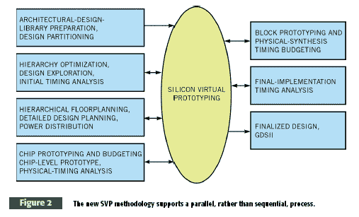
The new methodology supports a parallel, rather than sequential, process (Figure 2). The only way to get feedback on the physical characteristics of a circuit resulting from decisions you make during logic design is to start physical design at the same time as logic design. The parallel process provides designers with more accurate information as new logic is developed, allowing them to incrementally update the values of the physical parameters. The design team must be able to evaluate multiple alternatives for critical aspects of the design, such as global power-network topology, function-block layout, and bus structures. The parallel nature of the methodology requires that engineers must view and analyze parts of the design at whatever level of physical abstraction they need. Abstract models are sufficient when designers are performing chip-level planning and optimization. Designers need detailed levels of abstraction for critical blocks to attain the necessary accuracy to analyze those blocks. They need to use the prototype to drive the construction of the final implementation. The final layout stage must use the prototype as an input and complete the detailed placement and routing while continuously monitoring timing, area, power, and signal-integrity metrics.
When they receive a circuit netlist, traditional place-and-route tools try to determine the best location for a cell, given the shape, orientation, connectivity, and timing budget, while keeping track of the requirements for power routing and the clock tree. As the design grows and the complexities of the constraints increase, the job requires significantly more computing power and time. Doing such a job with a completely flat design is becoming impossible. Designers have adopted a hierarchical design method to handle the complexity. But the method is feasible only if it allows designers to obtain reasonably accurate feedback about the resulting placement and routing on the chip.
SVP is a way to quickly obtain an implementation of the physical design to evaluate design trade-offs and improve the project's implementation plan. Design teams use SVP to identify and prioritize performance and manufacturing issues so that development work can continue in an orderly and deterministic fashion. Correlation of the timing results between SVP and final place-and-route tools is critical. Designers can verify the correlation by feeding the result of the SVP into the place-and-route tool and comparing the final results with those that the SVP predicted. Good timing correlation relies on RC extraction, delay calculation, and timing analysis. Because engineers use the prototype for power-network planning and noise prevention and repair, they must also compare the SVP results with the measurements they obtained after the final layout. A new SVP tool has no value until actual results confirm its predictions. Engineers using SVP go through a number of steps and perform many functions in creating and refining the prototype. Designers begin the process by generating a netlist using a logic-synthesis tool. The netlist is functionally accurate, but simple wire-load models approximate the timing of the circuit. The creation of the actual prototype starts with the floor-planning of the chip.
The design team must take a hierarchical approach to designing the circuit so that they can reduce the design into manageable blocks and can work on as many blocks as they can handle concurrently. SVP also allows engineers to compare alternative chip-level plans. Designers can partition the design in different ways and build corresponding prototypes to analyze the physical characteristics of the various choices. Without SVP, engineers would have to wait until the physical implementation of a design was finished before evaluating its characteristics.
Engineers begin by placing blocks of cells that constitute a functional unit. They use their knowledge of each unit and its interface requirements to place the major design elements. SVP allows them to evaluate the benefits of physical partitioning and choose a partitioning scheme that places the least burden on design requirements. The SVP tool then automatically places the remaining portion of the design using a timing-driven algorithm. Designers then perform an RC extraction and timing analysis and follow them with optimization and clock-tree synthesis. If the results indicate that they have met their design objectives, this implementation becomes the basis for design refinements. The process optimizes each function unit in relation to its immediate feeder and consumer units until the placement, routing, and verification of adherence to the constraints has completed. Designers use the prototype for creating a netlist and implementing physical- and timing-design constraints for each block. They can then assemble the refined blocks in the design to check timing and physical closure. The process continues until it has optimized all of the blocks and the designers have met the design objectives.
SVP Handles Many Design Issues
The choice of process technology is important. Trad-itionally, designers always targeted the latest process available, but blindly choosing the most advanced process is now risky. A better choice might be an older, cheaper, higher yielding process, assuming that it can meet all design requirements. SVP helps designers to make the right choice. They start by constructing and decomposing chip-level timing, power, and area constraints to the block level. They analyze the chip-level timing to identify critical paths and use the block-level constraints for blocks in the critical path to drive the construction of the physical prototype. If the results of the analysis of the prototype are within constraints, they can proceed with the choice of process. If not, designers can explore another implementation alternative, such as using full-custom cells instead of standard cells, but they may also have to choose a different process. Multibit buses often require special measures and may even require changes to the architecture of the chip.
SVP helps designers visualize the impact of placement on connectivity. It is better to keep buses short, and, when this approach is impossible, it may be necessary to use a bus bridge to function as a repeater. This technique requires less power to drive the bus and thus minimizes the amount of noise the bus generates. Problems with excessive IR drop often remain undetected until engineers perform parasitic extraction and IR-drop analysis on the completed physical imple-mentation. In hierarchical designs, it is critical to derive block-level power budgets from chip-level requirements. IR-drop limits are always parts of such requirements. Designers use the budgets to drive the construction of the blocks. SVP helps in early detection of IR drop, because engineers can run analysis on the partial implementation of the design. Early detection of a problem area reduces the cost of fixing the design and provides a sound base for the next design step. In regions of the chip having many large macros, it is often difficult to place buffers on long nets, because the available space is insufficient. Engineers use SVP to visualize the placement and modify the problem areas by explicitly providing buffers in the netlist.
Hierarchical budgeting of timing constraints is a tedious, time-consuming, and error-prone task. Designers usually have to perform many iterations to resolve conflicts between the blocks and the top-level assembly. Rather than being a top-down process, timing information often passes from the bottom up from fully implemented blocks, causing irresolvable timing violations at the top level. SVP lets designers transform chip-level timing constraints into budgets for individual blocks and global interconnections. As designers develop and place blocks, SVP compares the timing of the implemented portion of the circuit with the overall budget. If these comparisons are satisfactory, they become the basis for establishing the budgets for the blocks and interconnections that designers still need to implement. If the results are higher than expected, engineers can optimize the circuit with a smaller database and a greater knowledge of the source of the cause than if they had to deal with the entire circuit.
Much of the consolidation in the EDA industry in the last couple of years has occurred in the IC-design market. Therefore, engineers have limited choices of vendors, and the products, in general, demand substantial yearly license pricesÑoften more than $250,000. The number of tools that vendors bundle into their products that support SVP justifies the price. You need at least six engines performing physical synthesis, timing and signal-integrity analysis, clock-tree synthesis, floorplanning, routing, power planning, and IR-drop analysis to accomplish all of the required tasks.
Other Tools
Cadence Design Systems introduced SOC Encounter in 2002. It combines SVP and detailed IC implementation into a unified system with a single-in-memory data model and user interface. Engineers that develop ICs with fewer than 10 million gates can use Nano Encounter, a cheaper version of the product. Encounter provides designers with a daily idea of the characteristics of the design in its silicon implementation. In addition to the engines in the general architecture, Encounter also provides a detailed nanometer routing engine with signal-integrity analysis. Customers can add other tools through the Encounter's API or through the OpenAccess database API. SI2 (www.si2.org) is making the OpenAccess an industry standard, and engineers can obtain the API and the database implementation directly from SI2.
Magma Design Automation provides a number of tools for SVP. Engineers that are developing designs without hierarchy can use Blast Create to synthesize, visualize, evaluate, and improve the RTL netlist, design constraints, floorplanning, and placement. Engineers designing more demanding chips that require the use of hierarchy can use Blast Plan. It partitions large designs into blocks and uses Magma's GlassBox abstraction technology to budget chip-level timing constraints among the top-level blocks. Both tools take advantage of the capabilities of Blast Fusion, a netlist to the GDSII chip-implementation system, which includes optimization, placement and routing, skew-clock generation, floorplanning, and power planning.
Monterey Design Systems supports SVP through its Calypso product. It combines hierarchical design planning, physical synthesis, and physical prototyping into a tool that uses a hierarchical database for design data. With Calypso, engineers can perform timing analysis and optimization, clock-tree synthesis, IR-drop analysis, block placement, port optimization, antenna fixing, and global routing. The product leverages the technology that the company deployed in IC Wizard, a hierarchical-design-planning tool; Sonar for physical synthesis and prototyping; and Dolphin for place-and-route functions.
The Galaxy Design Platform from Synopsys supports SVP with the integration of a number of point tools. It includes engines from Design Compiler, Physical Compiler, DFT (design-for-test) Compiler, Power Compiler, Floorplan Compiler, Astro, PrimeTime, TetraMax, starCXT, Hercules, and Proteus. The Milkyway database provides storage and a common schema for the design data. Engineers using Galaxy can perform feasibility analysis on the design by analyzing the design's performance, power, and area requirements. In the past, designers could use the engines in Galaxy only in a sequential manner. The platform lets them use the engines in parallel and evaluate the impact of a design choice at RTL on the physical implementation before completing chip layout.
Icinergy Software offers SOC Plan, which works with both Cadence and Synopsys SVP and synthesis products to provide engineers with the physical representation of a design. It enables architectural evaluation and provides a feedback on the impact of architectural choices. The product refines block placement and the aspect ratio of blocks in the design based on a set of user-defined targets and constraints. It also optimizes wire length, timing, and routing congestion within the block.
Hier Design brings the concept of SVP to the FPGA market. Its PlanAhead hierarchical floor-planner aims to reduce the number of iterations between logic synthesis and physical design. Designers can examine multiple what-if scenarios about the physical implementation of the design and fix potential problems before layout. Designers can group critical paths and modules to increase routability through connectivity analysis and usage control. The tool provides both manual and automatic partitioning and block sizing and placement, and it supports placement with clock-I/O and clock-region planning.
The percentage of chips containing some analog- or mixed-signal circuitry is increasing. Mentor Graphics has introduced ICassemble, which offers top-down-floorplanning, interactive-routing, and chip-assembly capabilities for analog- or mixed-signal circuitry. Designers of analog products can plan, implement, and connect blocks within a physical layout environment, thus shortening their design cycles. Although this method is not a literal equivalent to SVP for digital logic, it achieves some of the same goals by providing designers with a view of the physical implementation of the circuit at the block level. The view is useful in minimizing congestion and in managing wire lengths and critical signals.
Author Information
You can reach Technical Editor Gabe Moretti at:
1-941-497-9880
Fax: 1-941-497-9887
E-mail: gmoretti@edn.com
At a glance
The Industry Needs a New Approach
Engineers designing semiconductors using standard cells have always given precedence to logic functions over placement or interconnection. Designers think of functions first: They create products to perform functions. EDA tools also foster this approach, at least in the digital domain, by placing logic behavior before any physical characteristics of the circuit. Logic synthesis is a good example. Users must take care of any physical characteristic of the target circuit by specifying constraints and directives they use to refine the results, but the Boolean-logic equivalent of the functions the designer described at RTL drives the tool.
This approach served designers well until they reached the 180nm process. At that point, EDA vendors developed physical-synthesis products, but they, too, just try to massage the results of logic synthesis, albeit using better information than logic synthesis has. Now, even physical synthesis alone is insufficient. Statistics show that designers use only around 60% of the available die area for designs using 130nm. In theory, engineers using the latest process technology could place as many as 100 million gates on a die, but correctly connecting all of those gates is a challenging task. Too few 90nm implementations exist to produce meaningful statistics, but no reason exists to expect a greater percentage of gate usage; in fact, the percentage will likely be lower.
Designers will soon have at their disposal 250 million gates. They will need nine or more metal layers for power, clocks, and signals, multiple pitches between adjoining wires, via densities measured in the thousands per square millimeter, and pervasive use of flip-flop packaging to distribute thousands of I/O pins. At 130nm and smaller processes, you must prototype the silicon circuit to accurately measure the parasitic effects that impact the performance of the circuit. Dealing with interconnect issues is becoming difficult as you need to consider more physical variables. Designers must handle fabrication methods and the dynamic characteristics of conductors connecting two or more logic cells. Yet, the library that designers get from semiconductor vendors contains only logic cells. They must build connectivity on the fly using an increasingly complex set of rules. Engineers must work at correcting problems that often emerge during system-level design. Soon, placement and routing will displace verification as the most expensive part of a design.
However, this difficult approach is not the only one. Sufficient area is available on the die to change the approach. It is easier to fabricate regular structures than irregular ones. Memories and programmable logic are always the first commercial products to use a new process. Silicon vendors should make custom logic as similar as possible to regular structures. Instead of giving designers a blank expanse of silicon on which to build the circuit, they should give them a gridded silicon area. The grid would establish where they can place and how they can connect functional blocks. Suppose that designers could get a cell library that contains not only the logic blocks, but also the interconnect blocks.
A semiconductor vendor could provide cells for various lengths of interconnect, as well as cells that contain a number of parallel "wires." The bus cells could come with wires at different pitch values. The resulting distribution grid, providing for power, clocks, and signal distribution, transforms a bare die into a matrix that looks much like the unpopulated regular structure of an FPGA. Designers can now use a modification of the platform-based design method by aggregating function units with a high level of interaction into blocks. The collection of blocks forms the platform that designers will place on the grid. Designers would then work with a fixed grid for a layout that moves dynamically across the die area with the placement of each block.
Because designers can make connections only by using interconnect cells, a physical-synthesis tool could automatically respect the interconnection rules that the cell library establishes. Process rules will enforce spacing between adjacent interconnect cells to
explicitly avoid interference. Interconnection requirements and the available distribution grid determine the location of the placement of a new block. Every placement generates a set of possible interconnect grids. The set may be large, but it is finite, because the scheme does not allow custom interconnects. The final circuit is usually significantly smaller than the available die area, so the restriction on the characteristics of the interconnecting wires does not adversely affect designers' ability to develop the product. If this method is practical, its implications increase the importance of electronics system-level design.
Semiconductors vendors then must provide an interconnection library at the architectural level, showing the power requirements and the delay associated with the various types of interconnections available at the gate level. Engineers could then use a modified transaction-based simulator to evaluate chip timing early in the design process. The modification would allow engineers to assign delay and power-consumption values to each connection between blocks, but the transmission of a signal within the block would use only fixed delay values. The use of behavioral models of the blocks and propagation delays for each connection during the development of the product's architecture will provide a global view of the behavior of the design in the time domain. Simulation execution would take less time than do current methods, and engineers could simulate the design using available simulation languages.
Using this methodology would enhance the importance of connections in the design at the architectural level. By modifying the grouping of functions and the placement of the blocks, system architects directly impact the viability of the design. Hence, this method would provide them a direct feedback on the impact of architectural choices on the chip's functions. Designers using this approach would be able to address place-and-route problems at the architectural level. Architects using high-level wire models could avoid second-order parasitic issues before designing logic.
The availability of early analysis of the consequences of an architectural decision will help avoid costly redesign decisions when the design has reached the RTL or, even worse, when the gate level has grown too large to be practically manageable.
For more information on products such as those discussed in this article, go to www.edna-enq.com and enter the reader sevice number. When you contact any of the following manufacturers directly, please let them know you read about their products in EDN Asia.
|
Cadence Design Systems Hier Design Icinergy Software Magma Design Automation |
Mentor Graphics Monterey Design Systems Synopsys |
<!-- saved from url=(0044)http://www.ednasia.com/jan04/coverstory.html -->
![]()
|
|
|
|