|
 |
|
|
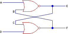
| This section gives a brief example of how a gate-level event-driven simulation might operate on the cross-coupled NOR gates of Fig. 6.5. |
|
In order to simulate the behavior of the circuit, a model of the behavior of each gate is needed. In simulating at the gate level, a truth table as shown in Fig. 6.6 is appropriate. Given the circuit and its functional behavior, only a test vector and a delay model are required to begin the simulation. Reasonable assumptions are that each gate requires a delay of one time unit, and that wires have a delay of zero time units. At time 0, all inputs and outputs are at logic value X. At some time t, input A is changed to logic value 1 and input D to 0.
The simulator then begins the algorithm given previously, which is repeated here:
| |||||||||||||||||||||||||||||||||
| FIGURE 6.6 Truth table for NOR gate. | |||||||||||||||||||||||||||||||||
Applying the test vector places two events on the queue:
This example focuses several important issues in simulation. A medium level of abstraction was chosen for this simulation. What are the implications of that choice? In simulating this circuit, about 10 events were processed. Even so, care was taken to avoid processing several events that had no affect on the circuit. In a circuit with several thousand gates, many hundreds of thousands of events might be processed. So it is important that the simulator is implemented efficiently, and that unnecessary events are not processed.
One way to avoid unnecessary event processing is to simulate with more abstract circuit elements. For example, we could replace the cross-coupled NOR gates with a two-input, two-output logic block the behavior of which is specified with a truth table. One line in the table indicates that inputs of 10 gives outputs of 01 after a delay of two time units. Simulating with this new logic block would result in only four events being processed (two for the test vector and two output events). This gives a faster simulation, but some information has been lost.
The NOR-gate simulation showed that the outputs actually settled independently: E changed to 0 at time t + 1, whereas F did not change to 1 until time t + 2. This information might have important implications, depending on the rest of the circuit, yet was not available when simulating with the more abstract circuit. The independent settling of the outputs is caused by the inclusion of feedback in the circuit, which is a common circuit-design technique. Feedback can cause many subtle timing problems, including race conditions and oscillations. As just demonstrated, the improper or unlucky choice of abstraction level can mask such problems.
Similarly, the NOR-gate simulation cannot model some types of behavior. It is well known that the simultaneous changing of gate inputs can lead to metastable behavior. The simple models used in this simulation cannot detect such behavior. A more detailed timing simulation or circuit-level simulation would be likely to find this type of problem, at the expense of time.
|
Previous |  |
Table of Contents | Next | |
Static Free Software |