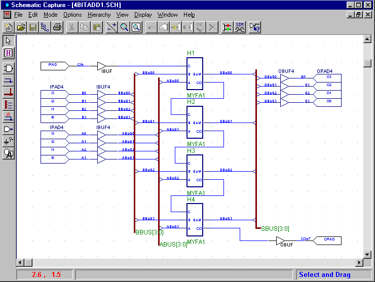
Figure 1: Top level schematic of the 4-bit adder (Screen clip from Xilinx (TM) Foundation software)
4-bit Adder
Hierarchical design and macros
Purpose:
The purpose of this lab is:
Pre-lab assignment:
In the previous lab you designed a full adder. In this lab you will use this module to build a 4-bit adder. In a next lab, you will include a 7-segment decoder circuit that will display the result in decimal form. The current lab assignment will focus on a 4-bit adder and the use of macros (hierarchical design methodology).
In-lab assignment:
A. Parts and Equipment:
You will build a schematic and simulate a 4-bit adder using the Full adder module (MYFA) that you designed in the previous lab.
- Open the Xilinx Foundation Tools. In the Project Manager, create a new project and name it MY4ADD. Place this new project in your own folder on the C:Drive (c:\users\your_name\) (and not in the Xilinx Project directory). Use the same procedure as you did for the creation of the last lab project (MYFA). If necessary, consult the tutorial. Select the proper family and part, depending on the board you will be using. For the Digilab board, select for family: Spartan XL, and for part: S10PC84.
- You will be making use of the last lab project (MYFA). You will need to copy last week's project (both the project folder and the .pdf file: MYFA and MYFA.PDF).
- Next, you need to add the full adder schematic (MYFA1.SCH) of last week's lab to the new project (MY4ADD). In the Project Manager window go to the DOCUMENT -> ADD menu. Type the full path name (C:\your _folder\MYFA\MYFA1.SCH if it is stored on the C:drive; you can also browse until you find the full adder schematic). The full adder schematic (MYFA1.SCH) should now appear on the left window pane (Files tab) of the Project Manager window.
- Now open the schematic editor: click on the Schematic Editor icon in the Project Manager window. Open the schematic for the full adder (MYFA) by going to the FILE -> OPEN menu in the schematic editor. Select MYFA1.SCH.
- The original full adder schematic will now appear on the screen. We will use this logic circuit of the full adder as a module in a larger schematic (4-bit adder). As a result, we do not want physical pins connected to each input. Thus you will need to replace the IPAD and IBUF for each input (A, B and C) by I/O terminals (if the difference between IPAD and I/O terminal is not clear yet, please refer to the tutorial on pads, buffers and pins; or consult the instructor). Do the following:
- Delete each IPAD and IBUF.
- Replace it with an I/O pin (terminal) by clicking on the terminal icon (Hierarchy connector) on the left side toolbar. When you place an I/O terminal you will be prompted for a terminal name in the I/O Terminal Window and to indicate if the terminal is an input or output. Give it the name A and for direction INPUT. Do the same for the other two inputs B and C.
- Also remove the OPAD and OBUF and replace them with I/O terminals as you did above for the inputs. However, specify as direction: OUTPUT (do not forget this!).
- When done, save the schematic (but do not close it yet).
- When the full adder schematic has been modified, you will need to create a macro.
- This is done by going to the HIERARCHY -> CREATE MACRO SYMBOL FROM CURRENT SHEET in the Schematic Editor window.
- A "Create Symbol window" will appear. Fill out the comment field (e.g. My full adder). You will notice that the Input and Output pins are listed. Check that all the pins are listed and that they are correct. If not, click on the CANCEL button and go back to the schematic. The input and output pins in a macro cannot be represented by PADs or Buffers. They need to be I/O termnals. (see 5 above).
- After creating the macro symbol you will be asked, "Do you want to modify it?" You can say NO (assuming that you already made the modification above).
- An empty schematic sheet will appear with the name MY4ADD.SCH. (If not, open a new sheet from the FILE menu in the Schematic Editor window). A sheet with the name MY4ADD1 will open. Now build the schematic for the 4-bit adder, using the previously created macro MYFA. Follow the same procedure as in the previous lab. Click on the Symbol Toolbox icon; you will see the newly created macro at the top of the window. You can now place the MYFA on the schematic. Then click on the MYFA symbol to place multiple copies (click ESC key to cancel).
- You can check that the MYFA symbol indeed represents your full adder circuit. Click on the H (Hierarchy icon on the left toolbar) and then double click on the MYFA symbol. The schematic of the full adder will appear. Go back to the top schematic MY4ADD.SCH
- Connect the full adders (refer back to your prelab) so that you end up with a 4-bit adder. The Carry output of the 1st adder should go to the carry-in of the 2nd adder, etc. Organize your schematic neatly in order to minimize the complexity of the connections. A neat schematic makes understanding its function and debugging much easier (also your grade will depend on it).
- The two 4-bit inputs (A3..A0) and (B3..B0) will be connected to the actual pins of the target device (FPGA or CPLD) on which you will implement this adder circuit (in a later lab). Therefore, you will need to add the IPADS and IBUFS on this top level schematic.
- Use the IPAD4 and IBUF4 symbols for the A and B inputs. Do not put the symbols too close together; there is plenty of space on your sheet. Do not connect the buffers to the inputs of the MYFA yet.
- Connect the outputs of the IPAD to the input of the IBUF and name the nets (using the names A0, A1, A2 and A3 for the A input and B0,...B3 for the B input (use the REPEAT function in the Wire Name window).
- Do the same with the outputs S0..S3. Also name the net for Cout (carry out of the last full adder).
- To connect the IBUF outputs to the inputs of the full adder modules, we will be using "Buses"in order to reduce the amount of wiring. Follow the tutorial on Top level schematic under Macros and Hierarchical Schematics. Give the buses an easy to recognize name (Ex. ABUS, BBUS, SBUS). See tutorial on how to use Buses (the use of buses can be tricky - read this section carefully). An example of a possible schematic is shown in Figure 1.
- Make sure all the input nets and output nets are named (the blue wires between the IPAD and IBUF).
- Save your schematic. Then go to OPTION -> INTEGRITY TEST; and OPTION -> EXPORT NETLIST.
- The next step is to do a functional simulation of the 4-bit adder. You will follow the same procedure as you did in the previous lab. Go to the Project Manager and click on Simulation button. Add your input and output signals first; then add the input stimuli. For the A0 input use the Bc0 output of the binary counter, for the B0 output use the Bc1 output, for A1 use Bc2, B1 use Bc3, etc. Connect the Cin (carry in) to a constant input of "0" by clicking on the 0 key (in the Keyboard section of the Stimulator Selection window). If necessary, read the tutoral on simulation.
- The simulation is basically the same as you did for the 1-bit full adder in the previous lab except for the presence of buses. Once you have assigned stimuli to the inputs you can collapse the buses. This is done by selecting the signals A0 to A3 and then going to the SIGNAL -> BUS -> COMBINE menu. The signal on the A bus will now be displayed in HEX form. Do the same for the B and S bus. This makes checking much easier. An example of a simulation is shown in Figures 2 and 3 with the buses collapsed and flattened, respectively.
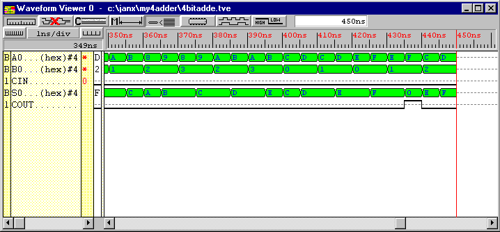
Figure 2: Simulation of the 4-bit adder with the buses collapsed for easy reading (Screen clip from Xilinx (TM) Foundation software).
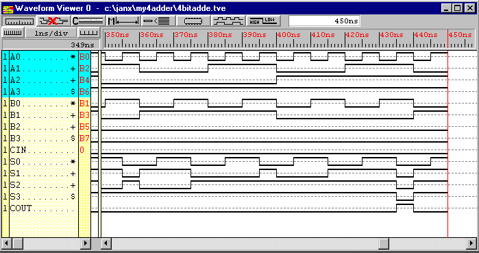
Figure 3: Simulation window of the 4-bit adder with the buses flattened (Screen clip from Xilinx (TM) Foundation software).
- Check that the output S0..S3 and Cout give correct values for the various input signals. If the simulation works correctly, put your names in the simulation window (Select the bottom signal in the Waveform viewer, ex. Cout; then go to WAVEFORM -> COMMENTS menu. Fill out your name in the comments window). Next, capture the screen of the waveforms and save it as a GIF file for insertion in your report. You can use the screen capture program (Hypersnap DX) that is installed on each PC.
- Capture the MY4ADD schematic (first put your name on it using the Graphics Tools) using Hypersnap DX.
- Save your project, and copy it to a zip disk or transfer it to another computer for use in the next lab. You need to copy both the project folder (MY4ADD) AND the .pdf file (my4add.pdf)! Without the .pdf file, you will not be able to open the project later on. An alternative is that you first archive the project (FILE-> ARCHIVE) from the Project Manager Window. This creates a zip file that you can easily move around. The zip file has all the information needed for the project.
Hand-in
You must hand in a short lab report that contains the following: