Digital Design Laboratory
Carry-Look-ahead Adder
Circuit Delays and Timing Simulation
Purpose
-
To Understand delays in digital circuits
-
To Learn to use the Timing Simulator
-
To Design a 16-bit carry-lookahead adder and measure its delay.
Background: Circuit Delays
Up to now we have been interested in the functional operation of logic
circuits. In the previous labs you used the logic simulator to verify that
the circuits function properly. However, there is one other important aspect
to circuit design: the speed at which it operates. The speed of a digital
circuit is very important, as it will determine the maximum frequency at
which it can work. Let us consider a PC that has a clock frequency of 800
MHz. That means that each 1.25 ns (i.e. period T=1/frequency) the PC will
perform a computation! As we will see, this will require clever circuit
design.
You may ask yourself what determines the speed or the maximum frequency
of a digital system? The answer is the delays of the circuits. There
are several factors that contribute to the delay. One is the propagation
delay due to the internal structure of the gates, another factor is the
loading of the output buffers (due to fanout and net delays),
and a third factor is the logic circuit itself.
-
Propagation delay
When the input signal of a gate changes, the output signal will
not change instantaneously as is shown in Figure 1 below.
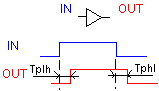
Figure 1: Propagation delay of gates
The propagation delay (or gate delay) of a gate is the time difference
between the change of the input and output signals. There are two types
of gate delays, TPHL and TPLH, as indicated in Figure1.
The value of the propagation delay varies from gate to gate and from logic
family to family. In general the more you are willing to pay for a device
(or chip), the faster it will be. The FPGAs we are using in the lab have
gate delays which vary between 1.5 and 4.5ns. The actual delay depends
on the way the logic gates have been mapped into the LUTs (Look up table)
of a CLB (Configurable Logic Block). The I/O buffers have delays in the
range of 2-4ns.
-
Fanout and net delays
The propagation delay described above is caused by parasitic capacitors
inside the gates and the physical limitations of the devices used to build
these gates. Another cause of delay is the capacitor associated with the
loads seen by a gate. These capacitors are the result of the wiring (net
delays) between gates (e.g. a long metal line connecting two gates on a
chip) and the input capacitor of the gates as is shown in Figure 2a.
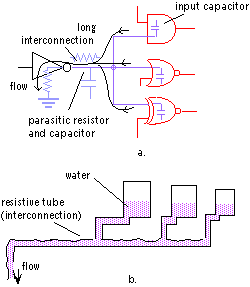
Figure 2: (a)Parasitic interconnection capacitors and fanout of a gate;
(b) hydraulic equivalent.
These capacitors need to be charged or discharged through the gate that
drives them (e.g. gate 1 in Figure 2a). The more capacitors that need to
be charged or discharged the longer it will take for the output to change.
Also, the longer the interconnection, the more resistance the nets will
have. The easiest way to visualize this is to use a hydraulic equivalent
of a capacitor and a resistor: a bucket filled with water and a narrow
pipe, respectively, as shown in Figure 2b. The more buckets connected to
the drain (i.e. the input inverter), the longer it will take to empty them.
This delay is the result of the fanout of the inverter.
-
Delay as a result of circuit topography.
Circuits that perform the same function can vary significantly in
their speeds. A good example is an adder circuit. The one you designed
in the previous lab is called a ripple-adder and is considerably
slower that a carry-look-ahead adder or CLA [1,3,4].
Measuring Circuit Delays
The overall speed of a digital system can be measured on an oscilloscope
by comparing the input to the output signals. However, during the design
phase, the circuit has not yet been fabricated and therefore, cannot be
measured. In that case it is possible to determine the delay of circuits
by doing a Timing Simulation. The advantage of a simulation
is that one can also determine the delay of internal nodes of a circuit.
This can be very helpful to understand which nodes or paths are the slowest
and thus limit the overall speed of the circuits. These paths are called
"Critical path". It is important to understand which paths are critical
in a circuit so that one can reduce their delay.
The actual delay will depend on how the gates have been implemented
in the various LUTs and CLBs. Also, the routing of the signals between
the different CLBs determines the overall speed. Thus, one needs first
to implement the design so that one can provide the Timing Simulator
with the block and routing delay information. The Timing Simulator and
the Implementation Tools are described in the tutorials.
Ripple-carry vs. Carry-look-ahead Adders
One type of circuit where the effect of gate delays is particularly
clear, is an ADDER. In this lab you will be measuring the delay of different
types of adder circuits. The 4-bit adder you designed and implemented in
the previous lab is called a ripple-carry adder because the result of an
addition of two bits depends on the carry generated by the addition of
the previous two bits. Thus, the Sum of the most significant bit is only
available after the carry signal has rippled through the adder from the
least significant stage to the most significant stage. This can be easily
understood if one considers the addition of the two 4-bit words: 1 1 1
12 + 0 0 0 12, as shown in Figure 3.
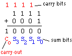 Figure 3: Addition of two 4-bit numbers illustrating the generation of
the carry-out bit
In this case, the addition of (1+1 = 102) in the least significant
stage causes a carry bit to be generated. This carry bit will consequently
generate another carry bit in the next stage, and so on, until the final
carry-out bit appears at the output. This requires the signal to travel
(ripple) through all the stages of the adder as illustrated in Figure 4
below. As a result, the final Sum and Carry bits will be valid after a
considerable delay. The carry-out bit of the first stage will be valid
after 4 gate delays (2 associated with the XOR gate and 1 each associated
with the AND and OR gates). From the schematic of Figure 4, one finds that
the next carry-out (C2) will be valid after an additional 2 gate delays
(associated with the AND and OR gates) for a total of 6 gate delays. In
general the carry-out of a N-bit adder will be valid after 2N+2
gate delays. The Sum bit will be valid an additional 2 gate delays
after the carry-in signal. Thus the sum of the most significant bit SN-1
will be valid after 2(N-1) + 2 +2 = 2N +2 gate delays. This delay may be
in addition to any delays associated with interconnections. It should be
mentioned that in case one implements the circuit in a FPGA, the delays
may be different from the above expression depending on how the logic has
been placed in the look up tables and how it has been divided among different
CLBs.
Figure 3: Addition of two 4-bit numbers illustrating the generation of
the carry-out bit
In this case, the addition of (1+1 = 102) in the least significant
stage causes a carry bit to be generated. This carry bit will consequently
generate another carry bit in the next stage, and so on, until the final
carry-out bit appears at the output. This requires the signal to travel
(ripple) through all the stages of the adder as illustrated in Figure 4
below. As a result, the final Sum and Carry bits will be valid after a
considerable delay. The carry-out bit of the first stage will be valid
after 4 gate delays (2 associated with the XOR gate and 1 each associated
with the AND and OR gates). From the schematic of Figure 4, one finds that
the next carry-out (C2) will be valid after an additional 2 gate delays
(associated with the AND and OR gates) for a total of 6 gate delays. In
general the carry-out of a N-bit adder will be valid after 2N+2
gate delays. The Sum bit will be valid an additional 2 gate delays
after the carry-in signal. Thus the sum of the most significant bit SN-1
will be valid after 2(N-1) + 2 +2 = 2N +2 gate delays. This delay may be
in addition to any delays associated with interconnections. It should be
mentioned that in case one implements the circuit in a FPGA, the delays
may be different from the above expression depending on how the logic has
been placed in the look up tables and how it has been divided among different
CLBs.
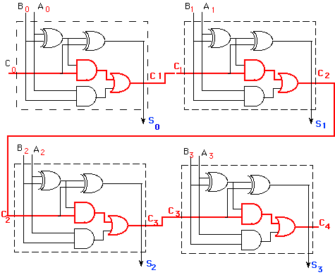
Figure 4: Ripple-carry adder, illustrating the delay of the
carry bit.
The disadvantage of the ripple-carry adder is that it can get very slow
when one needs to add many bits. For instance, for a 32-bit adder,
the delay would be about 66 ns if one assumes a gate delay of 1 ns. That
would imply that the maximum frequency one can operate this adder would
be only 15 MHz! For fast applications, a better design is required. The
carry-look-ahead adder solves this problem by calculating the carry signals
in advance, based on the input signals. It is based on the fact that a
carry signal will be generated in two cases: (1) when both bits Ai
and Bi are 1, or (2) when one of the two bits is 1 and the carry-in
(carry of the previous stage) is 1. Thus, one can write,
COUT = Ci+1 = Ai.Bi +
(Ai Å Bi).Ci.
(1)
The "Å" stands for exclusive OR or XOR.
One can write this expression also, as
Ci+1 = Gi + Pi.Ci
(2)
in which
Gi = Ai.Bi
(3)
Pi = (Ai Å Bi)
(4)
are called the Generate and Propagate term, respectively.
Lets assume that the delay through an AND gate is one gate delay and
through an XOR gate is two gate delays. Notice that the Propagate
and Generate terms only depend on the input bits and thus will be valid
after two and one gate delay, respectively. If one uses the above expression
to calculate the carry signals, one does not need to wait for the carry
to ripple through all the previous stages to find its proper value. Lets
apply this to a 4-bit adder to make it clear.
C1 = G0 + P0.C0
(5)
C2 = G1 + P1.C1 = G1
+ P1.G0 + P1.P0.C0
(6)
C3 = G2 + P2.G1 + P2.P1.G0
+ P2.P1.P0.C0
(7)
C4 = G3 + P3.G2 + P3.P2.G1
+ P3P2.P1.G0 + P3P2.P1.P0.C0
(8)
Notice that the carry-out bit, Ci+1, of the last stage will
be available after four delays (two gate delays to calculate
the Propagate signal and two delays as a result of the AND and OR gate).
The Sum signal can be calculated as follows,
Si = Ai Å
Bi Å Ci = PiÅ
Ci.
(9)
The Sum bit will thus be available after two additional gate delays (due
to the XOR gate) or a total of six gate delays after the input signals
Ai and Bi have been applied. The advantage is that
these delays will be the same independent of the number of bits one needs
to add, in contrast to the ripple counter.
The carry-lookahead adder can be broken up in two modules: (1) the Partial
Full Adder, PFA, which generates Si, Pi and Gi as defined by equations
3, 4 and 9 above; and (2) the Carry Look-ahead Logic, which generates the
carry-out bits according to equations 5 to 8. The 4-bit adder can then
be built by using 4 PFAs and the Carry Look-ahead logic block as shown
in Figure 5.
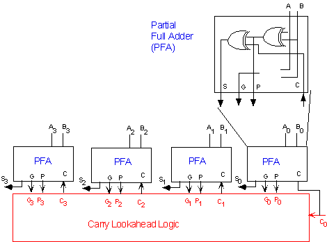
Figure 5: Block diagram of a 4-bit CLA.
The disadvantage of the carry-lookahead adder is that the carry logic is
getting quite complicated for more than 4 bits. For that reason, carry-look-ahead
adders are usually implemented as 4-bit modules and are used in a hierarchical
structure to realize adders that have multiples of 4 bits. Figure 6 shows
the block diagram for a 16-bit CLA adder. The circuit makes use of the
same CLA Logic block as the one used in the 4-bit adder. Notice that each
4-bit adder provides a group Propagate and Generate Signal, which is used
by the CLA Logic block. The group Propagate PG of a 4-bit adder
will have the following expressions,
PG = P3.P2.P1.P0
;
(10)
GG = G3
+ P3G2 + P3.P2.G1.
+ P3.P2.P1.G0
(11)
The group Propagate PG and Generate
GG will be available after 3 and 4 gate delays, respectively
(one or two additional delays than the Pi and Gi
signals, respectively).
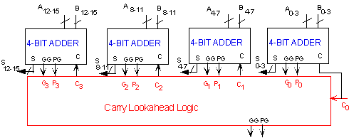
Figure 6: Block diagram of a 16-bit CLA Adder
Pre-lab assignment:
-
Describe briefly which factors determine the maximum frequency of a digital
circuit.
-
What is a critical path in a digital circuit?
-
Read the tutorial on "Timing
Simulation".
-
Assuming that one delay in a AND and OR gate is 1 gate delay
and in an XOR gate 2 gate delays, determine:
-
What is the worst-case delay of the Carry-out of the one-bit Full Adder
circuit of Lab 1
-
Consider the 4-bit adder you designed in the previous lab. Under what conditions
of input signals does the worst case delay occur for the carry-out signal?
What is the worst case delay for the carry-out (of the last stage)?
-
What is the worst case delay of signal S2 of a 4-bit ripply carry adder?
-
What is the worst case delay of signal C2 of a 4-bit ripply carry adder?
-
Assume you add two 16-bit words up using a ripple-carry adder. Considering
worst case conditions, after how long a delay will the sum (S) be valid?
-
What is the delay of the Sum bits S0 and S3 of the 4-bit carry-lookahead
adder in figure 5 above?
-
What is the delay of the Sum signals S3 and S15 of the 16-bit CLA in
figure 6 above?
- Submit your answers online using Blackboard.
In-lab assignment:
A. Parts and Equipment:
-
PC
-
Xilinx Foundation Tools F2.1i
B. Experiments:
-
You will implement a 16-bit carry-lookahead adder. You will
do this by creating a Partial Full Adder (PFA) macro and a Carry-lookahead
Logic macro as shown in Figures 5 and
6.
-
Create a macro for the Carry- Look-Ahead Logic block. Call this MYCLALOG.
Use VHDL to create this macro. You should also generate the Groups Generate
and Propagate signals, PG and GG, respectively. You
do not need to create the carry C4. Do a simulation, as explained above.
-
Now you can create a 4-bit CLA adder macro. In the schematic editor go
to the TOOLS -> SYMBOL WIZARD menu and create the symbol for a Schematic
macro, called MY4CLA. Once the symbol has been created, draw the schematic
for the 4-bit adder using the above defined modules of PFA and MYCLALOG.
The adder should have as input A[3:0], B[3:0], and CIN. The outputs are
S[3:0], PG, and GG. Be careful when connecting the
carry signals. Since this schematic will be used as a macro, you do not
need to add input/output buffers and pads. For single signals use a terminal;
and for the buses (ex. A, B and S), define the bus as "input" or
"output" bus (or select End Bus if the terminals have been defined already).
-
When finished, synthesize the macro and simulate the 4-bit adder. Verify
its operation and make a screen caption of the functional simulation waveforms
(only one page).
-
You are now ready to create the top level schematic of the 16-bit carry-lookahead
adder. Use the block diagram of Figure 6.
-
The schematic of the 16-bit adder is the top level schematic. All
the input pins (A[15:0], B[15:0], CIN, SOUT[15:0], and COUT) need to be
connected to pads and buffers. Cout is the last carry of the adder, corresponding
to C16 and can be generated from the groups Propagate and Generate signals.
-
In order to keep the schematic and its interconnections managable, use
buses as much as possible. It may be helpful to use a 16-bit wide bus for
input signals A and B. This bus can be split up into segments of 4 bits
that each feeds into the 4-bit inputs of each of the 4-bit CLA macros.
This can be done by first drawing a 16-bit wide bus (e.g. AIN[15:0]). Then
connect the 4-bit wide input bus (e.g. A[3:0]) of the first 4-bit CLA
to the 16-bit wide A bus; next connect the input of the 2nd 4-bit CLA to
the same A bus, etc. until all 16 inputs have been connected. Now you need
to specify how the bus signals are connected. This can be done by
giving the bus segment the proper name by clicking on the bus. This will
open the Edit Bus window. Keep the name but change the bus width. For instance,
to specify a 4-bit wide bus segment that connects to the input of the first
4-bit adder, give it the name AIN and as width [3:0]. It is important that
the name of the bus segment is the same as the name of the 16-bit bus.
Do the same for the other bus segments (e.g. AIN[7:4], etc.). For more
information about buses in the Schematic Entry window, select HELP -> SCHEMATIC
EDITOR HELP CONTENTS. In the help window select INDEX and type "buses"
or "bus connections".
-
When done, do a functional simulation and verify that the circuit works
properly. Instead of defining each input signal A0, A1 ... A15, B0,
B1, ... B15 separately, it is more convenient to use the Formulas to define
the input signals of the input buses. See section on Formulas
in the Logic Simulator Tutorial. When the simulation give the right result,
take a screen catpure of the waveforms (again only one page).
-
When the circuit works properly, you need to implement it so that
you can do a timing simulation later on.
-
Make sure you added pads and buffers for each input
and output. If you don't add pads, the mapping software will remove all
the logic between input and output "connectors" and your circuit will have
no logic or little logic left!
-
Before implementing the design, go to the Program
Manager and select the IMPLEMENTATION -> IMPLEMENT DESIGN menu (or ->OPTIONS
menu). In the Implement Design window click on the Option button.
When the Options window opens, click on the Edit Options button for the
Simulations (Foundation EDIF). In the Simulation Options window, click
on the General Tab and De-select the option: Correlate Simulation Data
to Input Design.
This will prevent that the timing simulation
will give undefined signals (see also undefined
signals in the timing simulation tutorial).
-
For the implementation, see previous lab or check the tutorial on Design
Implementation. Use a device speed of 4.
-
Check the reports and write the results in your lab notebook:
-
Check the Map Report for the device utilization and the equivalent gate
count. Check if logic has been removed during the mapping step.
-
Check the Post Layout Timing Report. Find the maximum combinational path
delay and net delay.Between which input pin and output pin does the maximum
delay occur? What is the maximum frequency at which the input signals
can applied without causing erroneous operation of the 16 bit adder?
-
Timing simulation (Verification): In the Project Manager click on
the Verification (Timing Simulation) icon. This will open the timing
simulator. Do a worst-case simulation of the CLA and determine the delay
of the Sum bits and the Carry out bit COUT. In case you
have problems with the timing simulation and some of the signals are undefined
(gray waveform), see the notes below. You do not need to go through
all the possible input combinations because you have verified that the
circuit works properly by doing a functional simulation above.
-
Apply input signals A[15:0] and B[15:0] which give a worst case scenario
for the delays of the sum and carry-out signals? Measure the delays between
the time the input signal is applied and the sum and carry-out signal changes
(use the measurement option in the simulator). Write these numbers down
in your lab notebook. Do they correspond to the ones reported in the Post
Layout Timing report?
-
When doing the timing simulation, be careful that the period of the stimuli
(i.e. the signals applied to the input) is larger than the longest delay
of the circuit. If your input signal is changing before the output signals
appear (due to the delay), you will get useless and unpredictible results.
You can change the period of the binary counter output (Bc:) by going to
the OPTIONS -> PREFERENCES -> SIMULATIONS; adjust the Clock Period of B0
to a value larger than the maximum delay (e.g. 50 ns). The input signal
should not change until all the output signals have settled to the proper
value.
-
Besides the delays of the Sum and Carry signal determine also the delay
of the input and output buffers.
-
Take a screen capture of the simulation data, including the measurement
data for the delays of the Sum, Carry-out and buffer delays (max 2 screens).
Notes:
-
In case some of the signals show as an undefined signal (gray
in the waveform viewer window or blue X on the schematic) make sure that
you De-select the option: Correlate Simulation Data to Input
Design in the Implementation Options (Simulations) as explained above
or in the timing
simulation tutorial.
-
Use the Measurement tool to determine the delay: go to WAVEFORM -> MEASURMENT
-> MEASUREMENT ON. This will allow you to display the delays.
Hand-in at the start of next lab:
Lab Report including
-
Course title, Lab no, Lab section, your name and date.
-
Section on the lab experiments:
-
Brief description of the lab including the goals
-
Copy of the VHDL source code of the macros PFA, MYCLALOG.
-
Screen capture of the schematic of the 4 bit and 16-bit CLA adders
-
Screen catpure of the funtional simulation of the 4-bit CLA adder (label
printouts)
-
Screen catpure of the timing simulation with measurements16-bit carry-look-ahead
adders.
-
Summary of the Map (device utilization) and Timing Reports (delays)
-
Discussion of the measured delays using the Timing simulator.
-
Maximum frequency at which the 16 bit CLA adder can be used.
-
Discussion and conclusions.
References:
-
R. Katz, "Contemporary Logic Design", Chapter 3, sections 3.3.1 and 3.3.2;
Chapter 5, section 5.2
-
D. Van den Bout, "The Practical Xilinx Designer Lab Book", Prentice Hall,
Upper Saddle River, NJ, 1998.
-
J. Wakerly, "Digital Design," 3rd edition, Prentice Hall, Upper Saddle
River, NJ, 2000.
-
M. M. Mano and C. R. Kime, "Logic and Computer Design Fundamentals", 2nd
Ed., Prentice Hall, Upper Saddle River, NJ, 2001.
Go to the Xilinx
Foundation Tutorial
Copyright 1999, Jan Van der Spiegel;
October 15, 1998; Updated by J. Van der Spiegel, October 10, 2001.