In this lab we will not be concerned with producing a compact layout; however, it is important that the layout be functional and design rule error free. We will be using the scn08hp technology for this exercise (lambda = 0.4U).
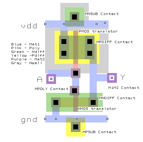
The goal of this lab is to introduce the student to CMOS layout via
the Led Editor. Your goal will be to produce a layout similar to the CMOS inverter
layout shown below:
In this lab we will not be concerned with producing a compact layout;
however, it is important that the layout be functional and design rule
error free. We will be using the scn08hp technology for this exercise
(lambda = 0.4U).
Make a directory for your work. Change to this directory and execute the command:
ln -s /ecad/local/tech/rel/gdt/scn08hp.dir/LedrcThis creates a symbolic link to the Led initialization file for the scn08hp technology. You should always do this for whatever technology you are assigned to work in. One of the things the 'Ledrc' file does is set the LED x,y grid to be equal to one-half lambda for the current technology; in this case lambda = 0.4U.
Start up Led by doing:
Led -t scn08hp -l /ecad/local/tech/rel/gdtExecute 'Cells -> Create New Layout Cell' to open a new layout cell. Name your cell 'myinv'. Creating a layout in Led uses the same editing commands as used for creating a schematic. Layout creation in Led involves connecting elements together; the elements you will be using are:
You can use
Display -> Plot a grid [g]to display a grid to help with spacing of elements. The 'Ledrc' file defines the x/y grid spacing as half-lambda. If you are zoomed too far out, you will get the message 'grid too fine'; use the 'zoom in' command ('2' hotkey) to see the grid.
SAVE YOUR WORK OFTEN while creating your layout; Led has
been known to crash!!!
Use the 'Add->Transistor (v)' command to add an NMOS transistor. You
will need to use the 'Alter' commands to reflect and/or rotate the
transistor so that the Ndiffusion runs horizontally and the drain
terminal is on the right side. Use the 'Alter-Size' command to set
the width of the transistor as specified here.
Place MNDIFF contacts on both the source and drains of the NMOS transistor ('Add->Contact (c)'). You MUST also add wires between the MNDIFF contacts and the respective source/drain terminals.
Wires are added to layouts using the same commands as used in
schematic editing (select an object, use 'A' to start the wire',
select the endpoint object). The type of objects selected for the
start/end points will determine the layer type of the wire. For
example, connecting a wire between an MPoly contact and a M1M2 contact
will use a MET1 wire; between a diffusion contact and a source/drain
terminal will use an NDIFF wire, etc.
You can also explicitly change the layer for a wire
via the 'Alter' command.
Add an MPOLY contact to the gate of the NMOS transistor as shown.
You MUST also add a wire between between the MPOLY contact and the gate
terminal of the NMOS transistor.
After adding the MNDIFF contacts, use the internal Led design rule checker on your cell via the :
Cells -> Rule Check Cells -> Chk. Current Cellcommand ('L' hotkey command). The Led Design Rule Check (DRC) is a quick DRC that will catch most errors; later we will use an external DRC program that will do a more extensive check. Any DRC errors found will be shown as cross-hatched boxes; use the 'Find->Jump to Next Error' command to cycle through the DRCs ('Ctrl-E' hotkey). Correct any DRC errors which have been detected. You should periodically do a DRC while you are editing; if you wait until you are finished with the entire layout before doing a DRC then you will find it more difficult to fix the errors because it may involve adjusting the spacing of many different elements.
Use the 'Add->Transistor (v)' command to add an PMOS transistor above the PMOS transistor. Check the design rules for spacings between NSUB (N-well where the PMOS transistor will be) to the NDIFF layer (which is part of the NMOS transistor). Use the 'Alter' commands to reflect and/or rotate the transistor to that the Pdiffusion runs horizontally and the drain terminal is on the right side. Use the 'Alter-Size' command to set the width of the transistor as specified here.
Place MPDIFF contacts on both the source and drains of the NMOS transistor ('Add->Contact (c)'). Set the width of the MPDIFF contacts to match the width of the PMOS transistor. You MUST also add wires between between the MPDIFF contacts and the respective source/drain terminals.
Add an MPOLY contact to the gate of the PMOS transistor as shown.
You MUST also add a wire between between the MPOLY contact and the gate
terminal of the PMOS transistor.
Add a MET1 wire to connect drain diffusion contacts of the PMOS and NMOS
transistors. This wire will connect the MNDIFF to the MPDIFF contact.
Add a MET1 wire that connects the poly contacts on the gates of the
two transistors together.
Add the M1M2 contacts as shown for the A and Y terminals. The M1M2 contact for the A terminal needs to be connected to the common MET1 connecting the PMOS/NMOS gate terminals (or connect it to one of the MPOLY contacts). The M1M2 contact for the Y terminal needs to be connected to the common MET1 connecting the PMOS/NMOS drain terminals (or connect it to one of the drain diffusion contacts).
Next, add a terminal of type 'IN' to the M1M2 contact used for 'A'. To add this terminal, first SELECT the M1M2 contact, then use the 'Add -> Add Terminal' command ('x' hotkey) to add the terminal. This should add the terminal node plus a wire which connects the terminal node to the M1M2 contact. Use the 'Alter' command to change the name of the terminal to 'A' and add a 'Viewname' property to make the terminal name visible.
Follow the same procedure to a terminal of type 'OUT' to the M1M2
contact used for the 'Y' terminal.
Add MET1 wiring as shown for the Vdd/GND rails. The VDD wire needs to
be added to the source diffusion contact of the PMOS transistor.
The GND wire needs to be added to the source diffusion contact of the NMOS transistor.
Add terminals of type VDD and GND to the wires; rename these terminals
to 'VDD' and 'GND' and make them visible.
Add MNSUB (Nwell plug), MPSUB (P-substrate plug) contacts as
shown. The MNSUB contact MUST be connected via a wire to the MET1 wire used for
VDD; the MPSUB contact MUST be connected via a wire to the MET1 wire used for
GND. Check the spacing rules for MNSUB, MPSUB contacts; the internal LED
DRC does NOT check all of the spacing rules for MNSUB, MPSUB contacts.
After your layout as has passed the internal Led DRC, execute the following command to run the external DRC:
mcDrGdt myinv.LThis program does a very detailed DRC on your layout. At the end of the DRC a message will be printed giving the status of the DRC; if there are errors, the message will refer to a text file which contains a description of the errors.
Once the layout has passed the external DRC, execute the following command to extract an hspice file for layout:
mcExtGdt hspice myinv.LThis program collapses the structures defined in the .L file down to their individual layers, then re-extracts the transistor and connectivity information based on the layer information. This is the 'acid test' of whether or not the geometric layers you put down actually form the circuit you desired. The output file will be called 'myinv.spice'; examine this file and verify that it does indeed form a CMOS inverter.
There is nothing to turn in for this lab. At beginning of the lab period when this work is due, the TA will ask you to demonstrate the following things: