Create a layout for the Dynamic D Flip-Flop, characterize
its operation, and verify that your cell can be used by AutoCells
inside of a standard cell layout.
You cell name must be 'ddrf301' (lowercase). The pin names must be D (data), CK (clock), R (reset), and Q. Note that pin names are upper case, while the cell name is lowercase.
Your spice simulations must meet the following requirements.
.tran .001ns 15ns
.option post nomod accurate
.global vdd gnd
Vvdd vdd gnd 5.0
Vr R gnd pwl 0n vdd_val, 0.05n 0, 2n 0, 2.05n vdd_val
In addition, all inputs (R, CK, D) must be buffered through an inverter in order to produce a realistic waveform shape at the input pins of the D-FF (D flip-flop). The linear slope produced by the 'pwl' function is NOT a realistic waveform shape for a CMOS circuit. I have provided an inverter model called 'invf101.sp' in the "reese/EE4253/project/scn08hp" directory that you need to use as the inverter circuit for all inputs.
This means that ALL measurements must be made at the input pins of the D-FF, NOT the input pins of the inverters. A common mistake is to measure the propagation delay from the input pin of the inverter to the Q output pin; this measures the propagation dealy of the inverter PLUS the D-FF; I want propagation delay of ONLY the D-FF.
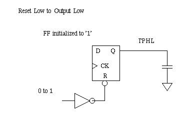
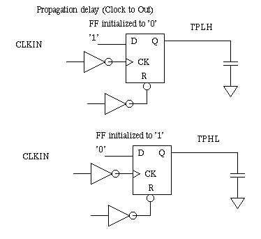
The first clock period should be used to clock in a '1'. Keep 'D' at a one, and apply a low true RESET signal in the clock phase just before the active edge (for rising edge triggered, when CLK=LOW; for falling-edge triggered, when CLK=HIGH). Apply the reset pulse at least 5 ns after the non-active edge of the clock in order to give transients a time to die down.
During the first clock period, reset your flip flop and have 'D' = '1'. On the first active edge, measure the prop delay of 'Q' going high. In the clock period, set D = '0'. On the 2nd active edge, measure the prop delay of 'Q' going low.
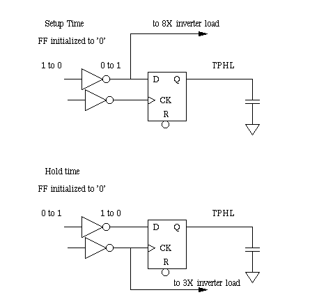
An additional circuit requirement for the setup time simulation is to place an 8X inverter load on the D input of the FF. This will give the D input a slow slew rate compared to the clock and provide a more pessimistic setup time. Use the 'invf101.sp' as the inverter. An '8X' load means that the inputs of 8 inverters must be tied to the 'D' input of the FF to simulate a fanout of 8X; the outputs of the inverters can be left open.
Measuring setup time or hold time requres a successive approximation approach. For setup time, I want you to report four numbers:
A common question is how long should you wait after the active clock edge for checking the Q output for success or failure - you can wait anywhere from 5ns to 10ns but no longer than this. For either your setup or hold, ONLY apply ONE ACTIVE clock edge to your circuit. Either your circuit will clock in the correct value OR IT WILL NOT. Make the pulse width of your clock long, and your transient analysis time long, and just check the Q output value at the of the transient analysis time. If the Q output was supposed to go to a '1', if it is not at least at the 70% point then it did not function correctly. If the Q was supposed to go to a '0', and it did not reach the 30% point, then it did not function correctly.
In my circuits, my transisent analysis time is 16ns with the active clock edge occuring around 8ns. I use the time before the active edge to use the 'RESET' input to initialize the flip-flop.
For the setup, hold offset parameters:
hold_offset_pass
hold_offset_fail
setup_offset_pass
setup_offset_fail
I want these to be simple offsets of the D waveform to the clock waveform - they do not have to 'measured' in any way. In my spice files I do:
VCK CK gnd pwl  0n CK_high,  8n CK_high,  8.05n CK_low
Vd  D  gnd  pwl   0n 0, '8n+hold_offset' 0, '8.05n+hold_offset' vdd_val
and
VCK CK gnd pwl  0n CK_high,  8n CK_high,  8.05n CK_low
Vd  D  gnd  pwl   0n vdd_val, '8n-setup_offset' vdd_val, '8.05n-setup_offset' 0
where hold_offset, setup_offset are defined as parameters (CK_high, CK_low are parameters as well whose values depend on whether it is negative triggered or positive triggered).
Of course CK, D pass through inverters before reaching the CK, D terminals of the ddrf301.
You can have NEGATIVE setup times; do not be surprised if this is true for your cicuit.
Hold time measurement is similar to setup time measurement. In this circuit, we want a 3X inverter load on the CK input of the FF (the D input of the D FF will just be tied to the driving inverter). This will give the CK input a slow slew rate compared to the D input and provide a more pessimistic setup time. Use the 'invf101.sp' as the inverter. An '3X' load means that the inputs of 3 inverters must be tied to the 'D' input of the FF to simulate a fanout of 3X; the outputs of the inverters can be left open.
For hold time, I want you to report four numbers:
You can have NEGATIVE hold times; do not be surprised if this is true for your cicuit.
The above diagram does not show R connected to any voltage source for brevity; you MUST have R connected to a voltage source.
The diagram below shows the HSPICE simulation setup for measuring input pin capacitance.

The diagram shows a measurement of the effective 'falling' input pin capacitance of the DUT (Device Under Test). The 'GI' source is a current-controlled current source (multiplication factor = 1) where the controlling current is the current measured by the Ammeter as shown. The 'C_fixed' capacitor can be any value, best results are obtained by a capactiance value in the PF range (use 10 Pf = 10e-12 for this project). The switches are implemented as voltage-controlled resistors. Switch B is CLOSED when the voltage at the input pin of the DUT is between 30% VDD and 70% VDD; it is open all other times. Switch A is the opposite of Switch B; Switch A is OPEN when the voltage at the input pin of the DUT is between 30% VDD and 70% VDD; it is closed all other times. HSPICE statements used to implement the ammeter, current source, and voltage-controlled resistors are given below (the hspice statements for the DUT, inverter, and voltage source for the input waveform are not shown!):
.param cfixed=1e-12
.param vdd_val = 5.0

vameter x y dc 0      ## the ammeter is between nodes X and Y, node Y
                      ## is the input pin of the DUT.  An ammeter is a
                      ## DC voltage source with value = 0

Gi a gnd CUR='i1(vameter)'
Ccb b gnd cfixed
Gra a gnd VCR pwl(1) y gnd 0,1e-15 1.49,1e-15 1.5,1e15 3.5,1e15 3.51,1e-15 5,1e-15
Grb a b VCR pwl(1) y gnd 0,1e15 1.49,1e15 1.5,1e-15 3.5,1e-15 3.51,1e15 5,1e15

.ic v(a) 0            ## make sure all voltages start at zero
.ic v(b) 0            ## make sure all voltages start at zero

.tran 0.001ns  7ns
.measure tran vc  max v(b,gnd)
.measure cpin param='(vc * cfixed)/(0.4*vdd_val)'
The measured pin capacitance is represented by 'cpin'. When
measuring the pin capacitance of one of the pins on your DFF, you
should ground the other input pins. Also, you need to measure both
FALLING and RISING pin capacitance for each input pin.
When you are calculating RISING edge pin capacitances, make sure to reverse the order of the reference nodes specified in the statement that 'captures' the maximum voltage across the cfixed capacitor:
.MEASURE tran vc max v(b,gnd)		;use this for falling edge
.MEASURE tran vc max v(gnd,b)		;use this for rising edge
Otherwise, you will get a vc=0 and cpin=0 b/c the voltage is negative in the rising edge calculation due to the current convention used by SPICE.
You will need to verify that your cell can be placed/routed within AutoCells. I have placed the following files in the project 'scn08hp' directory:
 Autocells.PAR
 batch.cmd
 bj_struct.R
 bj_struct.S
 build_lib.com
 lib.L
Look at the Autocells tutorial to review how to run AutoCells. I have already given you an Autocells Router file (bj_struct.R) so you DO NOT have to produce this file. You will need to run 'build_lib' before running 'Autocells'. After running Autocells and producing the final layout, there is one additional step that needs to be done. Assuming the final layout is in 'bj_struct.L', do:
/mpl/projects/cddd/tools/bin/notch_fill_sc.pl lib.L bj_struct.LThis will do notch and gap filling on your layout. Notches/gaps can form in various layers due to the layout/compaction process used by Autocells; these will produce false design rule errors. This script will automatically fill these notches/gaps. After doing this, run 'mcDrGdt' to perform a DRC on the final 'bj_struct.L'. You WILL get some design rule errors relating to MOSIS rule 8.5; these can be ignored (they will be listed as Rules 67, 68, 69, and 70). You may also get some errors pertaining to MOSIS Rule 4.4 (PSEL to NSEL spacing), these errors can also be ignored (the errors will show up as Rule 30, 31, 33, 34, 36). These errors are already present in the other cells referenced within 'bj_struct.L'. ANY other errors which are detected must be fixed.
This is the procedure I want followed for submitting project results:
    ddrf301.L        layout file
    ddrf301.data      data file containing your delay measurments
To submit the project to me, change to the directory above the 'final' directory, and do:
~reese/bin/submit_vlsi_project.pl
This will tar up contents of the 'final' directory and send it to me. It will also do some syntax checking on the 'ddrf301.data' file and abort with error messages if it finds a problem.
A sample 'ddrf301.data' file follows (I have provided a copy of this file in the '~reese/EE4253/project/scn08hp' directory):
########################################
# My ddrf301.data file
# each line has a key word and a value
# comment lines can start with '#'
# blank lines are ok
# ordering of key words is not important
# key words are case sensitive

ck_2_q_tplh  2.271e-10             # clock to Q  low to high prop delay
ck_2_q_tphl  3.979e-10             # clock to Q  high to low prop delay
reset_2_q_tphl 3.891e-10           # reset to Q  high to low prop delay


hold_offset_pass 160e-12           # see notes in lab10.html
hold_pass  90e-12
hold_offset_fail 120e-12
hold_fail 50e-12

setup_offset_pass 75e-12           # see notes in lab10.html
setup_pass  0
setup_offset_fail 35e-12
setup_fail -40e-12

d_pincap_fall 1.25e-14             # d pin capacitance for falling input
d_pincap_rise 8.4e-15              # d pin capacitance for rising input

ck_pincap_fall 1.08e-14            # ck pin capacitance for falling input
ck_pincap_rise 1.53e-14            # ck pin capacitance for rising input

reset_pincap_fall 1.29e-14         # reset pin capacitance for falling input
reset_pincap_rise 5.24e-15         # reset pin capacitance for rising input

############# end of ddrf301.data file ###############
You do not need to submit your extracted HSPICE file or the 'bj_struct.L' file that you placed/routed with AutoCells. I will extract the HSPICE file from your layout, and do my own place/route with your 'ddrf301.L' file.
You may want to check the your 'ddrf301.data' file yourself for syntax errors. Do this via:
~reese/bin/check_data.perl ddrf301.data
It will read your 'ddrf301.data' file and report the parameters it finds, and their values. It will notify you if parameters are missing.
Bob Reese
This is usually caused by not using the correct 'Ledrc' file when editing your ddrf301 or running Autocells. Your Ledrc file should be a symbolic link to
/ecad/local/tech/rel/gdt/scn08hp.dir/LedrcYou can create this link via:
% ln -s /ecad/local/tech/rel/gdt/scn08hp.dir/Ledrcinside of your 'scn08hp' directory.
Some people are trying to narrow the difference between their
'hold_pass/hold_fail', 'setup_pass/setup_fail' times down to
nearest picosecond.
This wastes time (other students are trying to use the workstations)
and is unrealistic. When you narrow the difference down to 75ps or
less, STOP. You have other things you can spend your time on and other
students need the workstation. It will not improve your grade to have
the interval down less than 75 ps.
Some folks are confused on whether to use 70% or 30% points
to measure setup and hold times at the 'D' and 'CK' pins on the
DFF.
It is JUST like propagation delay.
If D is rising, and CLK rising, then use 30% on D, 30% on Clk.
If D is falling, and CLK rising, then use 70% point D, 30% on Clk.
If D is rising, and CLK falling, then use 30% point D, 70% on Clk.
If D is falling, and CLK falling, then use 70% point D, 70% on Clk.
Whether or not D is rising or falling depends on whether or not you
are using one inverter or two inverters to buffer your D input signal
(some people are using two inverters so that they don't have to worry
about the signal inversion).
Whether or not Clk is rising or falling depends on whether or not you
have a rising or falling edge triggerred FF.
setup_fail, setup_pass are measured at the PINS of the FF, not at the
pins of the inverters driving these signals.
hold_fail, hold_pass are measured at the PINS of the FF,not at the
pins of the inverters driving these signals.
I think some folks are confused about what negative and positive
setup/hold times are.
setup time is the amount of time the D input must be stable before
the active clock edge in order to clock in the correct value.
If the D input can change AFTER the active edge and still clock in the
the correct value, then you get a negative setup time.
Assume you trying to clock in a '1'. Let D = '0'. If D has to change from '0' to
'1' before the active clock edge in order to clock in a '1', then you have positive
setup time. If it can change from '0' to '1' after the clock edge and
'1' still gets clocked in, then you have negative setup time.
hold time is the amount of time the D input must be stable after
the active clock edge in order to clock in the correct value.
If the D input can change BEFORE the active edge, and still clock in
the correct value, then you get negative hold time.
Assume you trying to clock in a '1'. Let D= '1'. If D has to change from '1' to
'0' after the active clock edge in order to clock in a '1', then you have positive
hold time. If it can change from '1' to '0' before the clock edge and
'1' still gets clocked in, then you have negative hold time.
Ignore errors 33, 36, 67,68,69,70. These are caused by other SCMOS library cells and are not errors that will cause a functional problem int the layout. If any other errors are present, they are caused by your 'ddrf301' cell interacting with neighboring cells and you must fix your 'ddrf301' cell to get rid of the errors. Do not edit the 'bj_struct.L' file and fix the errors there; edit 'ddrf301.L'.
If you are using a machine at EE in the CAD lab, DO NOT log into one of the ERC machines. This bogs down the person who is currently using the ERC machine. The Sparc5s in the ERC VLSI lab are not faster than the Sparc 5's at EE. Please show some courtesy.