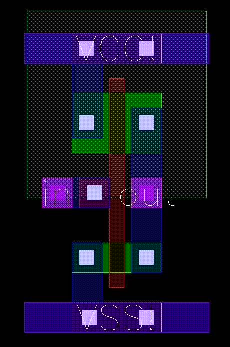
Do the layout for a CMOS inverter using the Cadence -Virtuoso tool suite. You can refer to this inverter layout.Use transistor sizes of 2.4u/0.6u for the PMOS transistor and 1.2u/0.6u for the NMOS transistor. Use a metal1 width of10 lambda for the power buses VCC and VSS. For this part, it is not necessary that your layout be compact but thelayout should be functional and design rule error free. We are using scn05hp technology for which lambda is 0.3u.
Part B: Design Rule Exercise
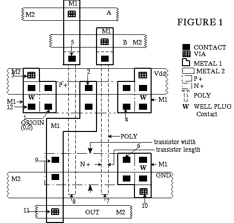
Figure 1 is a sketch of a CMOS circuit. Assume the minimum dimensions
from the MOSIS design rules -- unless otherwise noted below. Use W=12 lambda
and L=2 lambda for all transistors. Use a metal width of 8 lambda for the
power buses, Vdd and Gnd. Use a poly interconnect pitch of 8 lambda in
the channel region. Define the reference point at the center of the left
source contact of the PMOS transistor as shown. Problems 1-10: What are
the co-ordinates of the points indicated relative to the reference points
provided. The numbers refer to the center of the contacts of vias except
for #7 and #8 which refer to the end of the poly lines. Provide your answers
in terms of lambda.
| Problem | Coordinate # | relative to | Coordinate # |
| 1 | 12 | relative to | 1 |
| 2 | 2 | relative to | 1 |
| 3 | 3 | relative to | 12 |
| 4 | 4 | relative to | 1 |
| 5 | 5 | relative to | 2 |
| 6 | 6 | relative to | 4 |
| 7 | 7 | relative to | 6 |
| 8 | 8 | relative to | 7 |
| 9 | 9 | relative to | 6 |
| 10 | 10 | relative to | 6 |
To turn in:
1. A plot of your inverter layout for part A
2. Your answers to the design rule exercise of part B
3. A plot of the layout for part C
4. Answer to part D