


The designer of any new product must plan for testing at any time
in the life cycle of the product. This process is called design
for test (DFT). The test methodology, defined by the IEEE 1149.1
standard, is used to ease problems associated with both product
development and all levels of testing. Once boundary-scan architecture
is built into a device, tests developed for that device can be
reused after it is in a product. Figure 6-1 summarizes the concerns
applicable to any new product design.
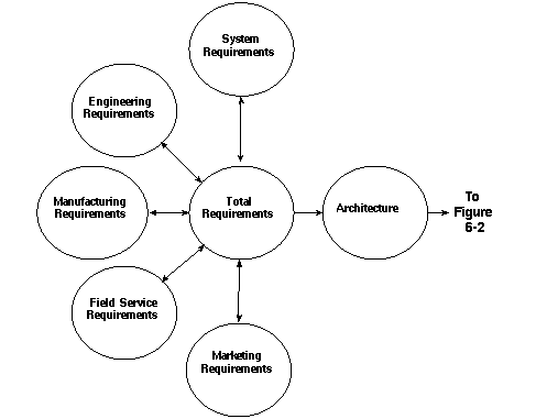
Figure 6-1. Initial DFT Concerns
Before implementing an boundary-scan test scheme, the designer must define test requirements for the following phases of the product life cycle:
These studies must ensure that the necessary controls are designed into the hardware to support the following requirements:
For both manufacturing test and field test, IEEE 1149.1 logic and test vectors can be used to test clusters or blocks of logic.
Internal IC testing at the board or system level requires a subset of the complete IC logic verification patterns to validate basic IC logic functions. Each level of hierarchical testing has a different set of fault characteristics. IEEE 1149.1 logic can be used throughout the testing life cycle of the product.
BIST usually consists of special circuitry built as part of an IC's internal design. BIST tests typically perform these functions:
IEEE 1149.1 commands can initiate BIST tests and return the test results.
Many high-density microprocessors and ASICs now include internal IEEE 1149.1-compliant scan circuitry. High pin count and fine-pitch packages limit physical access to package pins and devices with high gate count limit observation of the internal logic states. Internal scan, either partial or full, can do the following:
Internal scan also allows on-chip emulation control and circuit observability within a device to provide design verification. The emulation capability can also aid in software development to control highly complex functions designed into a device.
Figure 6-2 summarizes the various steps involved in ASIC and board
design.

Figure 6-2. Designing Testability for ASICs and Boards
Synthesis of ASICs has become a popular approach to ASIC design. ASIC designers faced with DFT for the first time are concerned about lack of knowledge and the additional design time involved. Today, there are several vendors supporting IEEE 1149.1 synthesis into ASICs. For example, the Synopsys Test Compiler family offers IEEE 1149.1 synthesis to generate these functions:
The compiler also automatically generates test vectors for IEEE 1149.1-compliant designs. This means that a designer can quickly and correctly implement basic IEEE 1149.1 test circuitry in an ASIC.
If synthesis is not available, most ASIC vendors offer a library of macros that the designer can use to implement IEEE 1149.1 into their designs. Using vendor macros requires considerably more effort and knowledge to implement IEEE 1149.1 into an ASIC compared to using synthesis. However, using vendor macros is significantly easier than implementing boundary-scan architecture using a library that has no such macros. Texas Instruments offers a family of IEEE 1149.1-compliant ASIC macros for gate array and Field Programmable Gate Arrays (FPGA).
The ASIC designer is required to provide a Boundary-Scan Description Language (BSDL) file that describes the finished ASIC. This information becomes the basis for tools that create board interconnect test vectors automatically. These vectors can be used by the board designer for debug and validation and by manufacturing test departments for quality assurance.
Several synthesis tool vendors plan to implement automatic BSDL creation that is available once the ASIC synthesis has been completed. The creation of a BSDL file by the ASIC designer is straight forward if the design tool used does not create it automatically.
During IC simulation, the designer can use the IEEE 1149.1 logic to simplify the simulation patterns required to validate the design. First, patterns must be developed to verify that the IEEE 1149.1 interface is operating properly. Simple IR and DR scan patterns can be developed to perform this check. If internal scan is implemented, then simulation pattern sets can be written to test internal logic clusters using the internal scan registers. This partitioned approach simplifies design validation.
Many IEEE 1149.1-compliant tools use SVF (serial vector format) as the primary test pattern data format and interfaces between simulators and ATE testers also support SVF.
A collection of manually-generated SVF patterns, simulation patterns translated into SVF and ATPG-generated SVF patterns can be used to validate the IEEE 1149.1 logic. Initial tests must first verify that serial data can be scanned into and out of the IC. Proper use of internal scan registers to partition the internal functional logic can simplify fault detection and isolation.
IC testing usually is broken into three parts; static functional tests at 1 MHz, at-speed functional tests, and parametric tests. Because IEEE 1149.1 architecture relies on serially scanning of control and test data, only static functional testing can be performed via the IEEE 1149.1 architecture.
INTEST patterns generated by a simulator can be used to
validate the internal logic of the IC. By comparing these patterns
with simulation results and by observing internal scan register
contents, the designer can isolate faulty internal logic. Figure
6-3 summarizes the design validation flow for all products, from
IC through system-level products.

Figure 6-3. Debug and Verification of a Boundary-Scan
Design
The board designer needs test data to use during the design debug and validation phase. This data includes:
The BSDL that the designer creates for the ASIC must be validated to ensure that it is correct since it will be used by tools that develop more tests for board debug and validation. The new tests are then applicable for manufacturing test and field service test vector generation. BSDL created by a synthesis tool should accurately reflect a device's construction.
Along with the BSDL file for the device, the ASIC designer may also be asked to provide a subset of the ASIC simulation patterns if the ASIC supports the optional INTEST instruction. A subset of the simulation patterns may consist of the static (1 MHz) functional patterns. The reason only a subset of patterns may be needed is because it may be impractical to reapply the entire static functional test pattern set at the board level. Many companies have found that they can achieve an acceptable level of confidence that the ASIC is functioning correctly using only a portion of the entire static functional pattern set.
Most of the concepts described for IC design also apply to board and system integration. BSDL is used to describe the IEEE 1149.1 scan architecture of an IC, and Hierarchical System Description Language (HSDL) is used to describe subsystems and systems. HSDL is used to describe the scan architecture, group discrete signals into logical groups (e.g., ADDR0 -15, DATA 0-7) and to define constraints.
A constraint defines a logic condition that can apply potentially harmful signals to a circuit. IEEE 1149.1 gives direct control of all scannable signals, so it is possible to create logic states that functionally would not be entered. For example, bus-arbitration logic can be overridden and dangerous hardware conditions or conflict can occur. An example of a constraint is to inhibit any test pattern that would cause two scannable output nodes to drive a common bus net at the same time.
At the board level, the designer must consider how to partition the IEEE 1149.1 scan path. Commercial devices are available (such as TI's SN74ACT8997(1) SPL) to switch a single primary scan path to one or more multiple secondary scan paths. The designer should consider the benefits and penalties associated with partitioned scan paths.
Penalties associated with partitioned scan paths include:
Benefits associated with partitioned scan paths include:
(1) SN54ACT8997, SN74ACT8997 Scan Path Linkers With 4-Bit Identification Buses, Literature Number SCAS157B, Texas Instruments 1994.
The IEEE 1149.1 architecture has the ability to detect, and in many cases, isolate a scan path fault. The Instruction Register definition requires that the two (2) least significant bits (those closest to TDO) of a device be a logic 1 followed by a logic 0 during an IR scan. This rule allows the IEEE 1149.1-compliant bus controller to perform a simple IR scan to prove all devices on the bus can drive a logic 1 and logic 0 on the TDI-TDO path. There are ATPG tools available that automatically generate SVF bus validation patterns that can be applied by the bus controller.
The primary objective of the IEEE 1149.1 standard is to allow control and observation of device input and output pins for the purpose of interconnect testing. The reduced size of IC packages has made interconnect testing of PWBs difficult and expensive when using conventional interconnect testing. Commercial tools such as Teradyne's VICTORY VIT (Virtual Interconnect Test) product develop SVF patterns for interconnect testing. VIT inputs the netlist and the BSDL of the scannable components and outputs an SVF pattern set. This pattern set along with a fault dictionary lookup table allows an IEEE 1149.1 bus controller to apply the interconnect patterns to the board and detect/isolate faulty interconnections.
After proving correct operation of the bus controller, the designer can control and observe all boundary-scan nodes. Tools such as ASSET allow interactive, macro, or C programming control for the designer. The board designer can also import and reapply the SVF patterns developed by the IC designer. This reuse of pattern sets provides these benefits:
The SVF pattern set developed by the IC designer tests an individual IC. The board designer has to be able to relocate the relative scan position of the IC SVF test to match its scan position on the board dynamically. Boundary-Scan software tools such as ASSET(tm) (Advanced Support System for Emulation and Test) allow dynamic test relocation.
As designers become better acquainted with IEEE 1149.1, they will no doubt find benefits well beyond those discussed in this chapter. The standard became available just in time to offer a solution and benefits to customers experiencing complexity problems introduced by new technology.
The benefits that customers can realize from IEEE 1149.1 architecture include:
TI Home
Search
Semiconductor Home