Boundary scan is a special type of scan path with a register added at every I/0 pin on a device. Although this requires the addition of a special test latch on some pins, the technique offers several important benefits. The most obvious benefit offered by the boundary-scan technique is allowing fault isolation at the component level. Such an isolation requirement is common in telecomunications switching environments where prompt field repair is critical.
A major problem driving the development of the IEEE 1149.1 boundary-scan standard is the adverse effect of surface-mount technology. The inclusion of a boundary-scan path in surface-mount components, in many cases, affords the only way to perform continuity tests between devices. By placing a known value on an output buffer of one device and observing the input buffer of another interconnected device, it is easy to see if the Printed Wiring Boards (PWB) net is electrically connected. Failure of this simple test indicates broken circuit traces, cold solder joints, solder bridges, or Electrostatic Discharge (ESD) induced failures in an IC buffer-all common problems on PWBs.
A less obvious advantage of the boundary-scan methodology is the ability to apply predeveloped functional pattern sets to the I/0 pins of the IC by way of the scan path. IC manufacturers and ASIC developers create functional pattern sets for DC test purposes. Subsets of these patterns can be reused for in-circuit functional IC testing. Reusing existing patterns in the development of system diagnostics can save large amounts of development resources, especially if many of the ICs in a system have embedded boundary-scan paths.
The IEEE 1149.1 standard is a common protocol and boundary-scan architecture developed into an industrial standard after thousands of man hours of cooperative development by approximately 200 major international electronics firms. Early contributors in the development of the IEEE 1149.1 standard were AT&T, DEC, Ericsson, IBM, Nixdorf, Philips, Siemens, and Texas Instruments. These companies recognized that only a nonproprietary architecture would encourage companies to offer the compatible integrated circuits, test equipment, and CAD software needed to bring product development, manufacturing, and test costs under control in today's competitive electronics marketplace. Many people believe that boundary-scan architecture will do for development, manufacturing, and test what the RS-232C standard did for computer peripherals.
Boundary scan is the application of a scan path at the boundary
(I/O) of ICs to provide controllability and observability access
via scan operations. In Figure 3-1, an IC is shown with an application-logic
section and related input and output, and a boundary-scan path
consisting of a series of boundary-scan cells (BSC), in this case
one BSC per IC function pin.
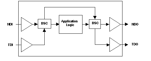
Figure 3-1. Boundary-Scan Example
The BSCs are interconnected to form a scan path between the host IC's Test Data Input (TDI) pin and Test Data Output (TDO) pin. During normal IC operation, input and output signals pass freely through each BSC, from the Normal Data Input (NDI), to the Normal Data Output (NDO). However, when the boundary-test mode is entered, the IC's boundary is controlled in such a way that test stimulus can be shifted in and applied from each BSC output (NDO), and test response can be captured at each BSC input (NDI) and shifted out for inspection. External testing of wiring interconnects and neighboring ICs on a board assembly is accomplished by applying test stimulus from the output BSCs and capturing test response at the input BSCs. As an option, internal testing of the application logic can be accomplished by applying test stimulus from the input BSCs and capturing test response at the output BSCs. The implementation of a scan path at the boundary of IC designs provides an embedded testing capability that can overcome the physical access problems in current and future board designs.
The IEEE 1149.1 architecture is shown in Figure 3-2. The architecture consists of an Instruction Register, a Bypass Register, a Boundary-Scan Register (highlighted), an optional User Data Register, and a test interface referred to as a Test Access Port (TAP). In Figure 3-2, the Boundary-Scan Register (BSR), a serially accessed Data Register comprised of a series of boundary-scan cells (BSCs), is shown at the input and output boundary of the IC.
The Instruction Register and Data Registers are separate scan paths arranged between the primary Test Data Input (TDI) pin and primary Test Data Output (TDO) pin. This architecture allows the TAP to select and shift data through one of the two types of scan paths, instruction or data, without accessing the other scan path.

Figure 3-2. Boundary-Scan Architecture
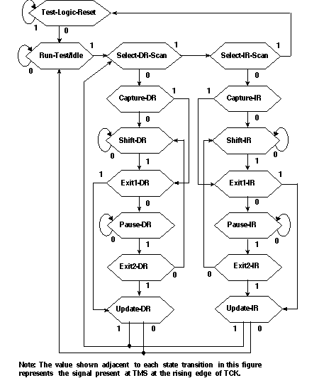
The TAP is controlled by the Test Clock (TCK) and Test Mode Select
(TMS) inputs. These two inputs determine whether an Instruction
Register scan or Data Register scan is performed. The TAP consists
of a small controller design, driven by the TCK input, which responds
to the TMS input as shown in the state diagram in Figure 3-3.
The IEEE 1149.1 test bus uses both clock edges of TCK. TMS and
TDI are sampled on the rising edge of TCK, while TDO changes on
the falling edge of TCK.
The main state diagram consists of six steady states; Test-Logic-Reset, Run-Test/Idle, Shift-DR, Pause-DR, Shift-IR, and Pause-IR. A unique feature of this protocol is that only one steady state exists for the condition when TMS is set high: the Test-Logic-Reset state. This means that a reset of the test logic can be achieved within five TCKs or less by setting the TMS input high.
At power up or during normal operation of the host IC, the TAP is forced into the Test-Logic-Reset state by driving TMS high and applying five or more TCKs. In this state, the TAP issues a reset signal that places all test logic in a condition that does not impede normal operation of the host IC. When test access is required, a protocol is applied via the TMS and TCK inputs, causing the TAP to exit the Test-Logic-Reset state and move through the appropriate states. From the Run-Test/Idle state, an Instruction Register scan or a Data Register scan can be issued to transition the TAP through the appropriate states shown in Figure 3-3.
The states of the Data and Instruction Register scan blocks are mirror images of each other adding symmetry to the protocol sequences. The first action that occurs when either block is entered is a capture operation. For the Data Registers, the Capture-DR state is used to capture (or parallel load) the data into the selected serial data path. If the BSR is the selected Data Register, the normal data inputs (NDI) is captured during this state. In the Instruction Register, the Capture-IR state is used to capture status information into the Instruction Register.
From the Capture state, the TAP transitions to either the Shift or Exit1 state. Normally the Shift state follows the Capture state so that test data or status information can be shifted out for inspection and new data shifted in. Following the Shift state, the TAP either returns to the Run-Test/Idle state via the Exit1 and Update states or enters the Pause state via Exit1. The reason for entering the Pause state is to temporarily suspend the shifting of data through either the Data or Instruction Register while a required operation, such as refilling a tester memory buffer, is performed. From the Pause state shifting can resume by re-entering the Shift state via the Exit2 state or terminated by entering the Run-Test/Idle state via the Exit2 and Update states.
Upon entering the Data or Instruction Register scan blocks, shadow latches in the selected scan path are forced to hold their present state during the Capture and Shift operations. The data being shifted into the selected scan path is not output through the shadow latch until the TAP enters the Update-DR or Update-IR state. The Update state causes the shadow latches to update (or parallel load) with the new data that has been shifted into the selected scan path.
In Figure 3-4, the TAP control output signals are shown along
with the Instruction and Data Register interconnects.

Figure 3-4. TAP Output Control Interconnect Diagram
This section contains descriptions of the required and optional registers specified in IEEE Std 1149.1-1990.
The Instruction Register is responsible for providing the address
and control signals required to access a particular Data Register
in the scan path. The Instruction Register is accessed when the
TAP receives an Instruction Register scan protocol. During an
Instruction Register scan operation the SELECT output from the
TAP (Figure 3-4) selects the output of the Instruction Register
to drive the TDO pin. A general Instruction Register architecture
is shown in Figure 3-5.

Figure 3-5. General Instruction Register Architecture
The Instruction Register consists of an instruction shift register and an instruction shadow latch. The instruction shift register (Figure 3-5) consists of a series of shift register bits arranged to form a single scan path between the TDI and TDO pins of the host IC. During Instruction Register scan operations, the TAP exerts control via the Instruction Register shift enable (SHIFTIR) and Instruction Register Clock (CLOCKIR) signals to cause the instruction shift register to preload status information and shift data from TDI to TDO. Both the preload and shift operations occur on the rising edge of TCK; however, the data shifted out from the host IC from TDO occurs on the falling edge of TCK. The status inputs are user-defined observability inputs, except for the two least significant bits, which are always 01 for scan-path testing purposes. (The Instruction Register has a minimum length of two bits.) When activated, the RESET* input sets the instruction shift register to be set to all ones. This forces the device into the functional mode and selects the Bypass Register (or the Device Identification Register if one is present).
The instruction shadow register (Figure 3-5) consists of a series of latches, one latch for each instruction shift register bit. During an Instruction Register scan operation, the latches remain in their present state. At the end of the Instruction Register scan operation, the Instruction Register update (UPDATEIR) input updates the latches with the new instruction installed in the instruction shift register. When activated, the RESET* input sets the latches to all ones.
The IEEE 1149.1 standard requires two Data Registers; Boundary-Scan Register and Bypass Register, with a third, optional, Device Identification Register. Additional user-defined Data Registers may be included. The Data Registers are arranged in parallel from the primary TDI input to the primary TDO output. The Instruction Register supplies the address that allows one of the Data Registers to be accessed during a Data Register scan operation. During a Data Register scan operation, the addressed scan register receives TAP control via the Data Register shift enable (SHIFTDR) and Data Register clock (CLOCKDR) inputs to preload test response and shift data from TDI to TDO. During a Data Register scan operation, the SELECT output from the TAP (Figure 3-4) selects the output of the Data Register to drive the TDO pin. When one scan path in the Data Register is being accessed, all other scan paths remain in their present state.
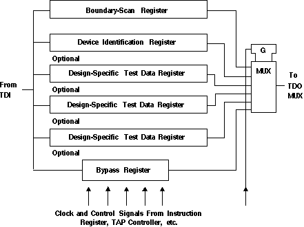
Figure 3-6. Test Data Register Architecture
Boundary-Scan Register - The Boundary-Scan Register (BSR)
consists of a series of boundary-scan cells (BSCs) arranged to
form a scan path around the boundary of the host IC. The BSCs
provide the controllability and observability features required
to perform boundary-scan testing as described in the Boundary-Scan
Overview section of this chapter. Shadow latches in the BSCs,
driving the NDO outputs remain in their present state during a
Data Register scan operation. At the end of a Data Register scan
operation, the Data Register update (UPDATEDR) input updates the
shadow latches with the new boundary test pattern to be applied
from the NDO outputs of the BSCs. Figure 3-7 shows a conceptual
view of a Control-and-Observe BSC.

Figure 3-7. Conceptual View of a Control-and-Observe BSC
Bypass Register (Required) - The Bypass Register consists of a single scan register bit. When selected, the Bypass Register provides a single bit scan path between TDI and TDO. The Bypass Register allows abbreviating the scan path through devices that are not involved in the test. The Bypass Register is selected when the Instruction Register is loaded with a pattern of all ones to satisfy the IEEE 1149.1 Bypass instruction requirement.
Device Identification Register (Optional) - The Device Identification Register is an optional register defined by IEEE 1149.1, to identify the device's manufacturer, part number, revision, and other device-specific information. Figure 3-8 shows the bit assignments defined for the Device Identification Register. These bits can be scanned out of the Identification Register after being selected.

Figure 3-8. Structure of the Device Identification Register
Although the Device Identification Register is optional, IEEE 1149.1 specification has dedicated an instruction to select this register. The Device Identification Register is selected when the Instruction Register is loaded with the IDCODE instruction, which is defined by the vendor.
Manufacturer's identification codes (Bit1 through Bit11) are assigned, maintained, and updated by the EIA/JEDEC office. Any company can be added to the JEDEC Standard Manufacturer's Identification Code (Publication JEP106) by request to the JEDEC office at 202-457-4973.
The IEEE 1149.1 standard defines nine test instructions. Of the nine instructions, three are required and six are optional. The following subsections contain brief descriptions of each required test instruction.
The required BYPASS instruction allows the IC to remain in a functional mode and selects the Bypass Register to be connected between TDI and TDO. The BYPASS instruction allows serial data to be transferred through the IC from TDI to TDO without affecting the operation of the IC. The bit code of this instruction is defined to be all ones by the IEEE 1149.1 standard.
The required SAMPLE/PRELOAD instruction allows the IC to remain in its functional mode and selects the Boundary-Scan Register to be connected between TDI and TDO. During this instruction, the Boundary-Scan Register can be accessed via a data scan operation, to take a sample of the functional data entering and leaving the IC. This instruction is also used to preload test data into the Boundary-Scan Register prior to loading an EXTEST instruction. The bit code for this instruction is defined by the user.
The required EXTEST instruction places the IC into an external boundary test mode and selects the Boundary-Scan Register to be connected between TDI and TDO. During this instruction, the Boundary-Scan Register is accessed to drive test data off-chip via the boundary outputs and receive test data off-chip via the boundary inputs. The bit code of this instruction is defined by the 1149.1 standard to be all zeros.
The following subsections contain brief descriptions of the optional IEEE 1149.1 instructions.
The optional INTEST instruction places the IC in an internal boundary test mode and selects the Boundary-Scan Register to be connected between TDI and TDO. During this instruction, the Boundary-Scan Register is accessed to drive test data on-chip via the boundary inputs and receive test data on-chip via the boundary outputs. The bit code of this instruction is defined by the user.
The optional RUNBIST instruction places the IC into a self-test mode, enables a comprehensive self-test of the IC's core logic, and selects a user-specified Data Register to be connected between TDI and TDO. During this instruction, the boundary outputs are controlled so that they cannot interfere with neighboring ICs during the RUNBIST operation. Also, the boundary inputs are controlled so that external signals cannot interfere with the RUNBIST operation. The bit code of this instruction is defined by the user.
The optional CLAMP instruction sets the outputs of an IC to logic levels determined by the contents of the Boundary-Scan Register and selects the Bypass Register to be connected between TDI and TDO. Before you load this instruction, you can preset the contents of the Boundary-Scan Register with a SAMPLE/PRELOAD instruction. During this instruction, data can be shifted through the Bypass Register from TDI to TDO without affecting the condition of the outputs. The bit code of this instruction is defined by the IC designer.
The optional HIGHZ instruction sets the three-state outputs of an IC to a disabled state and selects the Bypass Register to be connected between TDI and TDO. During this instruction, data can be shifted through the Bypass Register from TDI to TDO without affecting the condition of the IC outputs. The bit code of this instruction is defined by the IC designer.
The optional IDCODE instruction allows the IC to remain in its functional mode and selects an optional Device Identification Register to be connected between TDI and TDO. The Identification Register (see Figure 3-8) is a 32-bit shift register containing information regarding the IC manufacturer, device type, and version code. Accessing the Identification Register does not interfere with the operation of the IC. Also, access to the Identification Register should be immediately available, via a TAP data scan operation, after power-up of the IC or after the TAP has been reset using the optional TRST* pin or by issuing a Test-Logic-Reset instruction. The bit code of this instruction is defined by the IC device designer.
The optional USERCODE instruction allows the IC to remain in its functional mode and selects a User Data Register to be connected between TDI and TDO. The User Data Register is an optional 32-bit shift register containing user-defined information about the IC. Accessing the User Data Register does not interfere with the operation of the IC. The bit code of this instruction is defined by the IC designer.
To learn more about the IEEE 1149.1 standard, please refer to the publication, Standard Test Access Port and Boundary-Scan Architecture, IEEE Std 1149.1-1990 (includes IEEE Std 1149.1a-1993). This document is available through IEEE (1-800-678-IEEE, 908-981-1393), and is available on CD-ROM.
TI Home
Search
Semiconductor Home