 Figure 1: D-FF and Scan Structure Diagrams
By David E. Lackey
Note: This article has been submitted to 'Integrated System Design' for publication at some future date.
With continuing technical advancement in semiconductor manufacturing, the trend in the ASIC industry is toward ever-increasing chip density. This gives the product developer an affordable way to provide increased function and complexity in a highly integrated package. The need for design-for-test in ASIC products is growing in parallel with the density and complexity of the chips. Coupled with the increased density and complexity of the ASIC product is the complexity of testing combinational and sequential logic that is increasingly inaccessible to test equipment. How can product designers ensure quality in their product designs unless they can test this logic?
Scan-based design allows for more effective management of the increasing complexity of product test. It provides serial access to all registers that are inside the design, thus offering direct test access to all combinational and sequential logic.
An increasingly attractive ASIC design-for-test solution is Level-Sensitive Scan Design (LSSD). Used by IBM since the 1960s, LSSD is an effective and reliable way to use scan-based design-for-test, providing a basis for automatic test pattern generation (ATPG) and excellent diagnostic capability for hardware faults and design errors. LSSD also facilitates advanced design-for-test structures, including boundary scan, Built-In Self-Test (BIST) of logic and arrays, and IEEE 1149.1 test access capabilities. And, through various product design techniques, LSSD can also provide benefits to the product above and beyond design-for-test. Customers see improvements to product debug and performance, while providing flexible clock design. Further benefits from data capture, diagnosis, and improved product maintenance are by-products of the technique.
For IBM, LSSD has had a long track-record of success, realizing its benefits in products from IBM personal computers through the high-end ES/9000 (TM) mainframe, as well as microprocessor designs and ASICs. More recently, as IBM's role as a direct supplier of semiconductor technology in the global market has expanded, companies outside of IBM are seeing how LSSD is providing benefits to their products as well, and are increasingly embracing it.
Scan-based design, optimally implemented using LSSD, greatly reduces the complexity of product test and enables higher degrees of product quality. These benefits result in improvements to the product developer's competitiveness. The implementation of LSSD and scan, and their benefits to product development, are best understood by first reviewing a typical sequential logic design using edge-triggered D-FlipFlops.
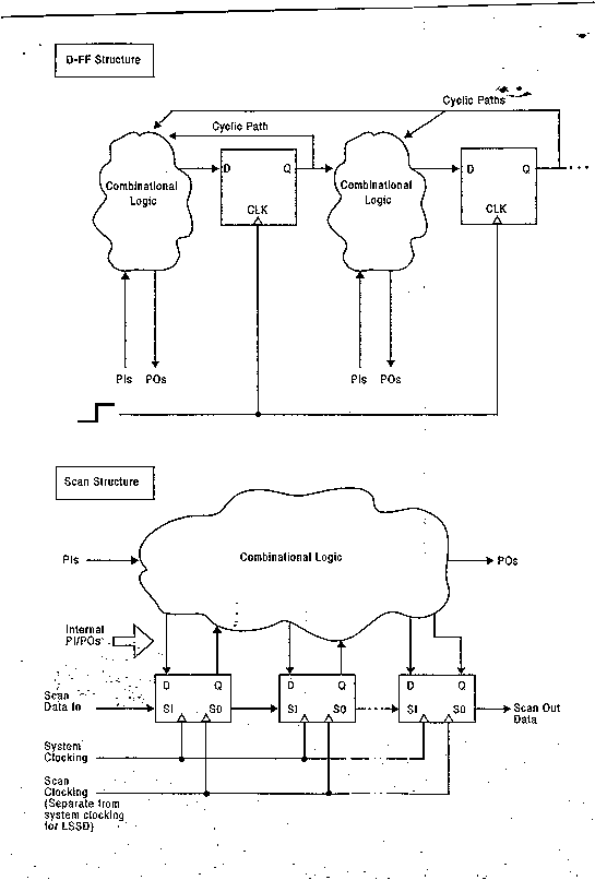
Every D-FlipFlop in the design captures the results of its preceding combinational function on the same edge (either rising or falling) of the clock, thus advancing the design to its next state.
While the D-FlipFlop and similar sequential design styles realize the benefits of synchronous design, it is, unfortunately, difficult to test as real hardware. Because the only external access to the combinational logic and the sequential elements is through the primary inputs (PI) and primary outputs (PO), the development of externally-applied test patterns to exercise a logic fault in the internal combinational circuits, as well as the sequential elements themselves, must account for the sequential and cyclic nature of the design. The result is a complex sequence of setup patterns required to apply the desired stimulus and subsequently observe the result.
Because of sequential and cyclic design, this complexity has proved to be a prohibitive problem for automatic test pattern generation approaches, and a nearly impossible problem for manual pattern development. As a result, product developers who decide on using D-FlipFlop or similar structures turn to functional test pattern development. It is fortunate that a subset of these tests sometimes overlaps those used for functional verification (simulation) and, thus, can be reapplied for manufacturing or product test. Traditionally, these functional verification tests achieve nearly 80 percent fault coverage. Unfortunately, higher levels of coverage necessitate the development of additional functional test patterns. The effort involved is tedious, consumes development resource, and extends the product development schedule on the order of months, while fault coverage improves to typically 90 percent, and sometimes 95 percent if a more extensive effort is applied. Product developers are often driven to purchase hardware accelerators to gain the simulation resources nessessary to ensure the correctness of these additional functional patterns.
The complexity of functional pattern development grows with increasing chip size and density, compounding the added development cost and further lengthening the product schedule. All of these factors result in impacts to the product developer's competitiveness.
Scan structures alleviate the need for functional patterns and enable automatic test
pattern generation by providing a serial data path to each sequential element, as shown in
Figure 1. In essence, each sequential element becomes a primary input and primary
output in the view of test pattern generation, and test complexity is reduced to the
testing of combinational logic. Fault coverage on the order of 99.5 percent or higher is easily
achieved using automatic test pattern generation software, with run times typically measured
in hours. Also, there are popular logic synthesis tools on the market today
that automatically insert scan capability into an existing D-FlipFlop or
similar structure.
Figure 1: D-FF and Scan Structure Diagrams
LSSD includes an optimal implementation of scan by
minimizing additional logic at the FlipFlop and
minimizing system data path delay because of scan. LSSD also
uses master-slave scan clocking, separate from the system clock, which eliminates scan's
inherent "early mode" timing exposure and generally allows for
the separation of system and
scan clocking issues.
These factors yield advantages for LSSD over typical non-LSSD
scan implementation, as shown
in Figure 2.
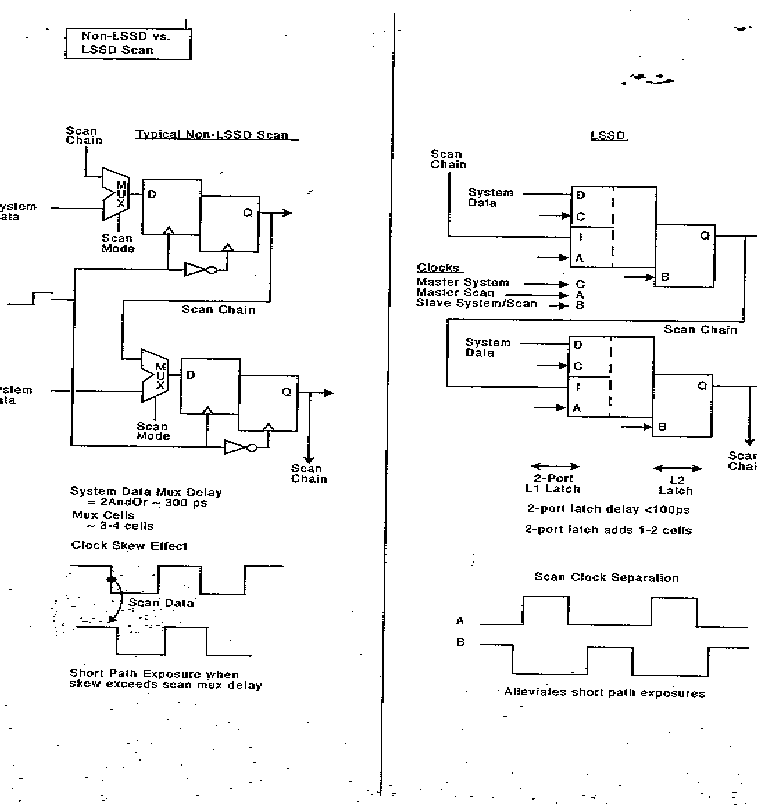 Figure 2: Non-LSSD vs LSSD Scan
LSSD can be used effectively within most design styles, fully realizing the benefits of scan-based design. The LSSD implementation, when used to its full potential, creates additional benefits in the product design.
Clock Design
Although LSSD is inherently a two-clock (master-slave) design method, it is easily achieved within a single-clock (edge-triggered) structure through the use of a clock splitter function. In system mode, the clock-splitter converts the single edge clock into system master and (opposite phase) slave clocks. In scan mode, the scan master and slave clocks are enabled instead. By placing the clock splitters late in the clock-powering tree, yet still sharing each clock splitter across several LSSD Shift Register Latches (SRLs), a high-performance clock structure is achieved while the additional logic per SRL is minimal.
LSSD can be used effectively with many other system clocking styles, including two-phase clocking, where two sets of level-sensitive latches are connected through combinational logic, and for sampling asynchronous interfaces.
Although capabilities exist to adapt LSSD to other clocking styles, LSSD provides additional benefits when its inherent master-slave clocking is fully utilized in the product design. LSSD clocking provides flexibility for adjusting, or tuning, the two phases of the clock to achieve maximum product performance late in the development cycle, as well as to provide flexibility during product debug. System master-slave clock overlap has often been used to achieve higher product performance by lengthening performance-limiting timing paths. The flexibility of adjustment and increased clock design options brings LSSD to the product developer as a way to achieve higher levels of product performance.
Sharing LSSD Pins
Although LSSD requires special primary inputs and primary outputs, design
techniques have been developed to allow each of these to be shared with
functional PIs and POs. It is possible to reduce the added I/O to a single "scan gate" PI
in situations where chip I/O constraints are their most severe. Figure 3
summarizes a few of these techniques.
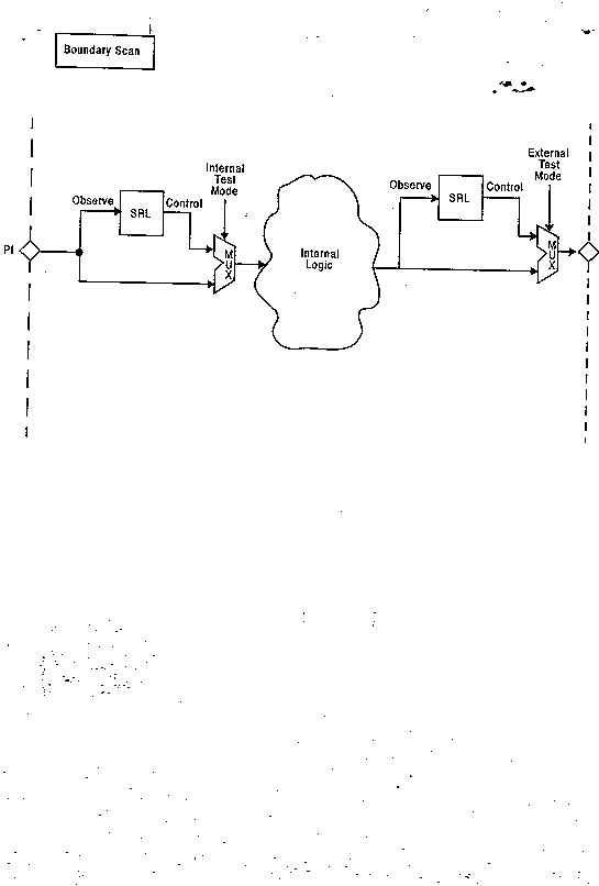 Figure 3: Pin Sharing Diagram
Asynchronous Set/Reset Design
Several methods of asynchronous set/reset design come with LSSD at no added hardware cost. One method sequences the scan clocks while applying a data sequence at the scan data inputs that maps to the desired initialization state of the SRLs. A second method, not requiring a unique data sequence to be externally applied, uses inversions in the scan chain at points where the initialization value from one SRL to the next changes in polarity. In this way, a constant (0 or 1) is applied at the scan data inputs, and the scan clocks are sequenced for at least the number of SRLs in the longest scan chain. A third method implements the scan chain as in the second method, but holds the scan clocks in their active state and lets the SRLs "flush" to their desired initialization states. Without LSSD, the product designer typically adds logic, either in the FlipFlop or in the combinational logic, to provide the set/reset function. With LSSD and any of the techniques described here, asynchronous set/reset already exists in the design and does not have to be added by the product developer.
Debug Capabilities
Invariably, a complex product requires special hardware "logging" features for product debug information, hardware operational status, field data capture, and the like. The scan capabilities of LSSD include the prerequisite hardware requirements of these features. Without scan, the product developer must add special hardware to meet these needs.
Are LSSD Costs Really Advantages?
When one considers the inherent advantages of LSSD in terms of these performance factors and built-in capabilities, and realizes that the most frequently-quoted "costs" of LSSD are performance and chip area overhead, one must ask whether these are truly costs or advantages!
There are several ways in which LSSD is used to test the design in the manufacturing process and in the product.
As discussed earlier, testing for logic faults is greatly simplified by LSSD's scan capability. The basic test consists of the following steps:
Both deterministic patterns and weighted-random patterns (WRP) are applied using this method. Deterministic patterns are generated by ATPG to exercise specific faults and are stored in the manufacturing tester during the test. In WRP testing, test patterns are generated randomly in the manufacturing tester during the test, while :hp1.weighting data,:ehp1. predetermined by ATPG, is stored. Weighting data creates a biased subset of an otherwise random pattern, reducing the time necessary to exercise those faults having a low probability of coverage using purely random data. The results of the test are compressed by the test equipment into a signature, which is compared to the signature predicted by ATPG. The benefit of WRP is a significant reduction in data that must be stored in the manufacturing tester.
Before running the above tests, patterns verifying correct operation of the scan logic are typically applied.
Logic Delay Testing
Testing for delay faults, or for faults only observable at the operating speed of the product, is an extension of the basic logic test described above. By programming the test equipment, the timing between the rising edge of the slave clock pulse and the falling edge of the next master clock pulse replicates the timing seen in the product at operating speed. ATPG produces additional test patterns to stimulate and observe "temporary stuck faults" after the rising and falling edges of the system clocks.
The testing of arrays embedded in the component under test is facilitated by a few simple (and, for the most part, nonconstraining) LSSD groundrules:
Boundary scan is a mechanism enabled by LSSD's scan capability, providing the following advantages for testing:
Figure 4 summarizes a basic implementation of boundary scan.
A variation of the boundary scan method described here is the IEEE 1149.1 boundary scan standard. This variation encompasses the boundary scan capabilities described above, plus an on-product test access port of 4 to 5 pins supporting the boundary test sequence. IEEE 1149.1 can be supported in, and is indeed a natural extension of, the LSSD framework because of its reliance on the scan capability of the boundary logic. The integration of LSSD and IEEE 1149.1 boundary scan, supported in popular design synthesis tools, is another example of how LSSD can be extended for product-level benefit.
By building on the capabilities of LSSD, more advanced design-for-test structures become possible. One of these is built-in self test (BIST), in which methods exist for testing both logic and arrays in both the manufacturing and product environments. BIST reduces the data storage requirements and control complexity of the manufacturing tester and product software by moving much of the test pattern generation and test sequencing into the product hardware.
In logic built-in self test (LBIST), a pseudo-random test methodology is used, as shown in Figure 5. A pseudo-random pattern generator (PRPG) is built into the product, which steps through a series of random patterns. Each bit of the PRPG is stepped into a separate scan chain for each random pattern. Once all the SRLs in the scan chains are loaded (with random data), the system clocks are activated. A new state, based on the SRL random data and the combinational logic, is captured back into the SRLs, containing the test results. The SRLs are shifted into a multiple input shift register (MISR), which compresses the resulting data into a signature. The signature is then unloaded and compared with a signature predicted by ATPG to determine whether a failure was encountered.
In array built-in self test (ABIST), address stepping, data generation and prediction,
and test control mechanisms are
built into the product, as shown in Figure 5.
The array under test is accessed (written and read)
using the address stepper and the generated data, and the resulting array data is
compared against the predicted data. A hardware indicator is activated in the event
of a failure.
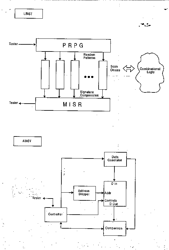 Figure 5: LBIST and ABIST Diagrams
In component manufacturing, these self-test functions are activated and controlled by the manufacturing test equipment. With the help of additional controls built into the product, these functions can be used in the final product as well. The provision for built-in self test in the IEEE 1149.1 specification (including the RUNBIST instruction) is an example of self-test control hardware implemented in the product. .pa
In addition to providing an optimal solution to the problems of defect-testing in the component and the product, LSSD can be used as a design vehicle for many other product advantages. Asynchronous set/reset, described earlier, is one of these. High-performance clock design is another. LSSD can also be used to reduce the time it takes to debug the design, improving time to market, and can be used to improve the management of product failures in the field, improving customer satisfaction.
Even with the best efforts applied to design verification (including functional simulation, static timing, and timing simulation), a number of design errors often "escape," and must be discovered and analyzed in prototype hardware. This is where one of scan's key benefits comes to play. At one or more points before the error, hardware "snapshots" are unloaded using scan. Because this scan data represents the machine state(s) in which the error occurs, isolation and determination of the failing product scenario comes quickly. In one particularly successful technique, a hardware snapshot is loaded into a simulation model of the product, and the simulator is then used to debug the problem. The result of debug using scan is a decrease, often in days or weeks, in the time needed to debug a design problem first seen in prototype hardware. When considering the full set of design errors to be debugged using prototype hardware, scan-based debug results in a significant decrease in time to market.
With the above capabilities, LSSD lends itself to additional debug requiremements, such as controlling the clocks for single-cycle operation, access to special hardware controls for "stop on event," and the ability to disable a failing hardware function and continue other testing in the presence of the error.
Over a complex product's life in the marketplace, failures may occur, whether because of latent design errors or as predicted in the defect rate of the silicon or packaging. The customer's satisfaction with the product is affected greatly&mdash.not so much by the occurrence of the error, but by the product down-time because of the error. This down-time is usually determined by how well the product design handles the error at the time it occurs.
Over the years, LSSD scan, LSSD clocking, and error-detection logic have been used successfully in complex system products to stop the clocks immediately after an error occurs, and scan out all product state data related to the detected error. This data is used immediately in a number of ways:
LSSD scan, together with product design, can yield a degree of concurrent maintenance capability. While the remainder of the product is running, the functional element under repair might be running scan-based diagnostics to gather additional information about the failure. After the FRU replacement, scan-based tests are run in the functional element to ensure proper logical operation. Upon completion, the product is reconfigured to utilize the functional element, bringing the product back to full, nondegraded operation.
When comparing non-scan and scan solutions, and LSSD and non-LSSD implementations of scan, it becomes clear that scan has significant advantages over non-scan. Scan solutions improve test coverage and, thus, improve hardware quality, improve time to market through test pattern automation and faster hardware debug, reduce cost for test pattern processing and test equipment, and provide an enabling path to self test, IEEE 1149.1, and other enhanced design-for-test structures. It also becomes clear that LSSD-based design is an optimal scan solution by providing better system performance through minimized delay in the system data path, more reliable scan clock design, and design methods that achieve the benefits of scan at minimal hardware overhead.
To facilitate a comparison, several design parameters are considered:
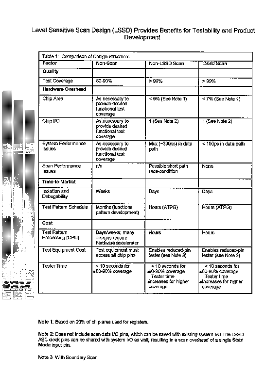 Table 1: Comparison of Test Method Benefits
Because LSSD is adaptable to many diverse system design styles, providing a path to design-for-test for most existing synchronous designs, it offers a stepping stone to many product benefits, including:
With increasing chip size and density, the need for design-for-test solutions is growing. Scan-based design is an effective answer to that need, and LSSD is an optimum implementation of scan with a long record of successful products behind it.