BIST Modeling and Its Application in Design Verification


Massoud Shadfar and Zainalabedin Navabi

Electrical and Computer Engineering Department
Faculty of Engineering, Campus No. 2
University of Tehran
14399, Tehran IRAN

Tel: +98-21-800-9215; Fax: +98-21-646-1024
Email: navabi@ece.ut.ac.ir


Abstract

Built in self test (BIST) has been used for testability of digital systems. VHDL modeling of BIST, not only can evaluate circuit under design for its testability, it can also be used for top-down design verification. This paper describes a VHDL modeling strategy for register level description of BIST. We will show how a BIST architecture inserted into a top level design can become useful in the lower level implementation of upper level components of a design. The paper will show application of the technique develop to a simple RISC architecture.


1. INTRODUCTION

A BIST VHDL description inserted into a behavioral description of architecture of a design can be used for modeling a testable final hardware [1, 2]. As with the other parts of a circuit, the BIST hardware is designed and simulated and finally implemented along with the rest of the circuit. The VHDL implementation and the model of the BIST hardware, therefore, will be useful for test and simulation of the complete circuit.

In addition to treating BIST as part of a hardware that can facilitate testing of the implemented hardware, it can also be used as a tool for design verification in the process of design implementation. The BIST model can help verifying the implementation of a behavioral model in a top-down design process. Simulation of the behavioral description of a design which includes a BIST controller and data registers, can yield a good circuit signature. This signature and the BIST hardware model can still be used to verify the operation of the circuit under design even if the original behavioral descriptions of the components of the design are replaced by models corresponding to their hardware implementations. Because a signature of the good operation of the hardware is available, low level gate or dataflow simulations will only need to apply test data leading to this signature. This will eliminate many simulation passes at low abstraction levels.

This paper describes a design process that uses a BIST architecture at high design abstractions for generation of a signature and uses this signature for verifying lower level design steps. We will describe the details of our suggested design process that can < p>can take advantage of BIST hardware for verification. Section 3 describes the verification method suggested by this methodology. Section 4 presents the BIST architecture used here. We will describe the workings of the BIST data registers and controller. Section 5 presents the VHDL modeling of the BIST as in Section 4, the registers and controller will be discussed. Section 6 presents an example hardware in which this design and verification methodology has been used.


2. DESIGN PROCESS

In a top-down design process, a behavioral description of a system is first described. After the RTL level design, the system model will consist of an interconnection list of component models. Each component model is at the behavioral level, which can further be broken into its sub-component. The process of partitioning an upper level design into its sub-component continues until a manageable set of parts have been reached.

Figure 1. Tool based design steps

Implementation of a design begins by bottom-up wiring of appropriate user designed or library cells. At each step of this design implementation, proper functioning of the gate level components must be verified.

It is best if the gate level implementation of each components is simulated along with other components and a unique test pattern is used for testing various levels of a components description, as well as the entire system. This same test pattern can later be used for production testing.

Figure 1 shows a design flow that uses VHDL simulation tools, gate level schematic capture tools, and layout editors and routing and placement programs. Specific tools that we have used in our design flow are suggested in this figure. The Vsim simulator of MTI is used for the behavioral and architectural level simulations. Gate level translation is the next step in the design process. This can be done by synthesis tools, or, at the component level, by schematic capture tools such as Orcad. Full custom implementation of the gate level netlist can be done by mapping circuit gates with their corresponding layouts from specific vendor libraries. At each design step simulations are performed to verify correct translation from one level of abstraction to another and also to generate more detailed information about the functionality of the circuit. Size information, power consumption, circuit speed and other physical properties of the final circuit will not be known until its layout is completed.


3. VERIFICATION PROCESS

A BIST hardware model inserted into an architecture model of a design will be able to generate appropriate good-circuit signatures and is instrumental in the test pattern design. When an behavioral level component is replaced by its gate level equivalent, this same test pattern and signature can be expected to verify correct gate level implementation of the component. A design begins with a correct VHDL architectural level model of a system. VHDL BIST models can easily be inserted into this model to generate a simulatable model for generating pseudo random test vectors, applying tests to components of the architectural level description, and signature calculations. Using a VHDL simulator, test patterns are generated by various types of BIST PRPG ( Pseudo Random Pattern Generator). These vectors are applied to the components of the architecture and their response will be used in the formation of a signature that represents the correct functioning of the system.

Figure 2 shows the various ways that an upper level description of a system is used in the first stages of the design. A behavioral level (Instruction level architectural description of the system) description is translated into a more hardware oriented description of interconnection of function blocks such as registers and logic units. This description is tested for proper execution of the system instructions (middle branch in Figure 2). The same description is used in a testbench for clock level simulation and calculation of a characterizing signature (for the specified test running time). This same description of the system is then used in still another testbench (left edge in Figure 2) for calculating the fault coverage of the calculated signature [3]. The process of calculating a signature and its corresponding fault coverage may be repeated until a signature with acceptable fault coverage is obtained.

Figure 2. Initial processings on upper level descriptions

As the design progresses, architectural level component models are replaced by models representing hardware implementation of each component. The signature obtained by the simulation of the behavioral model, can now be used for verifying this gate level implementation. In our proposed verification process, a unique test bench can be used to verify the gate level implementation, or a mixed behavioral / gate-level description of a system. This scheme helps isolate gate level parts of a system for diagnostic proposes.

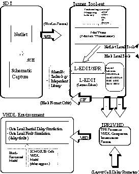
Figure 3. Extracting VHDL model from schematics

For mixed gate-level / behavioral simulation in VHDL, exact VHDL models for each of the gate level components must be obtained. Figure 3 shows the process used for this purpose. We have used a schematic capture program to design system components. The format obtained here is used in a placement and routing program that is part of the Tanner layout tool-set that we are using. Using a standard CMOS library a layout of the input netlist is obtained. A .TPR file contains the information on cell interconnections and a .CAP file contains the extracted capacitance information. Using a retargetting program, the .TPR and .CAP files are converted into an instantiation list of VHDL SCMOS cell models. The complete VHDL file is now simulatable along with other parts of the design that may be at the behavioral or netlist level. Programs for various file format conversions have been developed as part of our design methodology development.


4. BIST ARCHITECTURE

BIST architectures add extra test hardware to a design in order to reduce the test cost. Such a hardware performs test generation and evaluation of test results. A BIST architecture consists of test pattern generators, test response compressors and a BIST controller [4]. A common technique for test pattern generators and test response compressors is based on various types of LFSRs. We have used the Circular Self Test Path (CSTP) BIST architecture that consists of a circular path of registers and a controller [5]. Basics of each part will be discussed here.


4.1. Circular Path

The CSTP BIST architecture is a low cost BIST technique. In this technique a circular register path is formed by using the original system registers and possibly new test registers, as shown in Figure 4. Parallel inputs and outputs of this circular register are used for system and test data transfers to the other parts of the design. When in normal (system) mode of operation, system data are passed through register and busses of Figure 4. When the circuit is put in the test mode, same busses are used for loading parallel data into the data registers. The registers are now acting as MISRs (Multi-Input Scan Register) and responsible for data compression. In the test mode, the registers are also acting as PRPGs (Pseudo-Random Pattern Generator) for the generation of test data to the remaining parts of the design [6]. While the circuit is in the test mode, with each clock pulse a data compression takes place and a new test vector is prepared.

Figure 4 . CSTP architecture


4.2. CSTP BIST Controller

The circular path is controlled by the BIST controller to perform system operations, initialization, scanning or testing. In the system mode the additional test hardware is transparent to the design. At the beginning of a test, the BIST controller initializes the circular path to a known state. While in the test mode the circular path performs test pattern generation and test response compression. A final signature is obtained and is present in the circular path when appropriate number of clock pulses have been applied to the circuit in the test mode. Verification of the operation of the system can be done by evaluating contents of all or part of the circular path. The part being evaluated is now treated as a final signature of the circuit. Figure 4 shows R1 being used in the BIST controller for signature evaluation. The BIST controller is implemented as a state machine and it issues control signals to the registers of the circular path.


5. BIST VHDL MODEL

The CSTP BIST architecture VHDL model consists of a controller and several register models that are linked together to form the circular path register. Control and the data parts are linked by control signals issued by the controller. These signals place the circular path registers into various modes of operation.


5.1. Register Models

Each register of the circular path is described at the behavioral level, and includes control signals for operating at various system and test modes. Figure 5 shows the VHDL description for a typical circular path register. Circular path registers can be put into one of four possible modes. The modes are system, initialization, test and scan, and are controlled by the two bits of test_signal. In the system mode the registers function normally and load in their parallel inputs. In the initialization mode the registers are set to zero. This is important because the state of the circuit must begin from a known state in order to generate a pre-calculated signature. In the test mode, parallel data inputs and the register contents are compressed and are placed back into the register. The scan_in input and scan_out output are used for chaining registers in the CSTP path.


5.2. CSTP Controller

The CSTP controller consist of several control signals and a state machine. The state machine, shown in Figure 6, has 6 states for system mode, initialization, first test session, first evaluation, second test session, and second evaluation. The states are named sys, ini, tst1, comp1, tst2 and comp2 and are the enumeration elements of a the state enumeration type.

In the system mode, the test hardware is idle and the system is operating in its normal mode. In the initialization mode all storage cells are reset to zero. It is only important that a fixed value is initially loaded into the registers. This value must be the value based on which the good signature has been calculated. In this implementation we have used initial values of zero for all registers. In the first test session (tst1), 216 clock pulses are counted. With each clock a new test pattern is applied to the circuit and a new compression takes place. At the end of the count, in the first evaluation state (comp1), the contents of part of the circular path is compared against a pre-calculated signature. In our implementation the mar24 register contents are compared against X"0FFA25". If a match is found, the controller continues to perform the second test session. Otherwise, error is reported and the done flag is raised. If the first test session succeeds, the controller moves into tst2 state in which another 217 test applications and compressions take place. Following this state the comp2 state evaluates the results.

To reduce the probability of error masking, circuit signature is evaluated in two stages. This two stage evaluation is implemented in the controller state machine by tst1, tst2, and comp1, comp2 states.


    ENTITY instruction_register IS PORT (parallel_in : IN d_word; parallel_out : OUT d_word; load, clk, reset, scan_in : IN qit; scan_out : OUT qit; test_signal : IN half_nibble); END instruction_register;

  --

    ARCHITECTURE behavioral OF instruction_register IS BEGIN PROCESS ( load,parallel_in,clk, reset ) VARIABLE content : d_word; BEGIN CASE test_signal IS WHEN system => IF load = '1' AND clk = '1' THEN content := parallel_in; END IF; IF reset = '1' THEN content := zero_32; END IF; WHEN initialization => IF clk = '0' AND clk'EVENT THEN content := zero_32; END IF; WHEN test => IF clk = '0' AND clk'EVENT THEN content := compression (parallel_in, content, scan_in); END IF; WHEN scan => IF clk = '0' AND clk'EVENT THEN content := scaning (content, scan_in); END IF; WHEN OTHERS => NULL; END CASE; parallel_out <= content; scan_out <= content (content'LOW); END PROCESS; END behavioral;


Figure 5. CSTP register model


    ENTITY bist_controller IS PORT (reset, clk, start : IN qit; done, pass_fail : OUT qit; test_signal : OUT half_nibble; mar24 : IN qit_vector(23 DOWN TO 0); END bist_controller;

  --

    ARCHITECTURE behavioral OF BIST_controller IS BEGIN PROCESS . . . VARIABLE current : state; BEGIN CASE current IS WHEN sys => test_signal <= system; IF start = '0' THEN . . . . . current := sys; ELSE current := ini; END IF; WHEN ini => test_signal <= initialization; done <= '0'; pass_fail <= '0'; WAIT UNTIL clk = '0'; count := 0; current := tst1; WHEN tst1 => test_signal <= test; WAIT UNTIL clk = '0'; IF reset = '0' THEN count := count + 1; IF count = 65536 THEN current := comp1; ELSE current := tst1; END IF; ELSE current := sys; END IF; WHEN comp1 => . . . . . . . . IF mar24 /= X"0FFA25" THEN sig_bit := qit2bit_vector(mar24); write(ls,sig_bit,left,5); writeline(monitor1,ls); done <= '1'; pass_fail <= '0'; current := sys; ELSE current := tst2; END IF; count := count + 1; ELSE WAIT UNTIL clk = '0'; count := count + 1; END IF; WHEN tst2 => WAIT UNTIL clk = '0'; IF reset = '0' THEN count := count + 1; IF count = 131072 THEN current := comp2; ELSE current := tst2; END IF; ELSE current := sys; count := 0; END IF; WHEN comp2 => IF reset = '0' THEN IF mar24 /= X"C1275F" THEN . . . . . . . . . . . ELSE done <= '1'; pass_fail <= '1'; END IF; WAIT UNTIL clk = '0'; current := sys; . . . . . END CASE; END PROCESS; END behavioral;


Figure 6. CSTP Controller


6. APPLYING BIST TO A RISC PROCESSOR

Figure 7 shows a simple RISC CPU in which a CSTP BIST architecture has been inserted [7]. Selected CPU registers have became part of the BIST architecture. In the test mode these registers are responsible for random test pattern generation and compression of component outputs.

As shown, 24 lower bit of MAR register outputs are fed into the controller in order to be compared with the circuit signature. In addition to circuit registers, the circular path also contains the control signals of the processor.

The complete CPU shown here has been designed, simulated and verified using the methods presented in Sections 2 and 3 of this paper. Tools depicted in Figure 1 have been used in the design of this processor.


Figure 7. CSTP architecture implemented in the RISC CPU architecture


7. CONCLUSIONS

We have presented methodologies for the design and verification of VLSI circuits. VHDL based tools are used in this process. Where needed programs for linking VHDL based tools and other VLSI tools have been developed. The paper has presented the use and implementation of a BIST architecture. This architecture not only is useful for final testing of the circuit, but it is also used for verifying design steps leading to the VLSI implementation of a relatively large design.


Reference

[1] Armstrong, J. R. , " Chip-level Modelingn with VHDL," Prentice-Hall Inc. , Englewood Clif , N. J. , 1988.

[2] Z. Navabi, VHDL: Analysis and Modeling of Digital Systems, McGraw Hill, New York, 1993.

[3] V. D. Agrawal, " Sampling Technique for Determining Fault Converge in LSI circuits ", J. Digital sys., vol. V, no. 3, 1981, pp. 189-202.

[4] P. H. Bardell, W. H. MacAnney, J. Savir, "Built- In Test for VLSI: Pseudorandom Techniques", Jon Wiley&Sons, 1987.

[5] A. Kraniewski, S. Pilarski, " Circular Self-Test Path: A Low Cost BIST Technique for VLSI Circuits," IEEE Trans. on CAD , pp. 46-55, 1989.

[6] K. Kim, D. S. Ha, and J.G. Tront, " On Using Signature Registers as Pseudorandom Pattern Generators in Built-in Self-testing, " IEEE Trans. on CAD, Vol. 7, N0. 8, pp. 919-928, August, 1988.

[7] Patterson , D. A. , 1985 , " Reduced Instruction Set Computers." Communications of the ACM, Vol . 28(1), 8-21.