New VHDL Based Critical Path Tracing Method for
Fault Simulation


Massoud Shadfar, Armita Paymandoust, and Zainalabedin Navabi

Electrical and Computer Engineering Department
Faculty of Engineering, Campus No. 2
University of Tehran
14399, Tehran IRAN

Tel: +98-21-800-8485; Fax: +98-21-688690
Email: navabi_z@irearn.bitnet


Abstract

This paper presents a new method of critical path tracing for fault simulation. The details of this method, called one-pass critical path tracing, and its implementation in VHDL will be presented here. One-pass CPT is achieved by use of VHDL models for basic logical gates. By communicating via their ports, gate models a netlist will report faults that are detected on their ports due to application of test vectors at their primary inputs.


1. INTRODUCTION

A method of fault simulation is critical path tracing. In this method a test is applied to a circuit and detected faults are reported. This is opposite to the fault simulation in which a fault is inserted in the circuit and various tests are applied until one is found to detect the fault. While critical path tracing (CPT) is very useful for test grading, it cannot be used for fault dictionary generation.

After applying a test vector, the present CPT methods find a critical path that leads to the output of the circuit, and declare faults on this path as detected by the test vector. Fanout stems are only marked as critical when values assigned to the stems are found to influence the output. This is done by partitioning the circuit and performing simulations on sub-sections of the circuit. Obviously this process requires a preprocessing of the circuit as well as iterative evaluation of node values by use of simulation.

We eliminate the required preprocessing and iterative simulations of CPT methods in a new CPT method called, One-Pass CPT. After propagation of values corresponding to a test vector, all critical values will be determined by evaluation of the circuit in one pass from the output to the input of the circuit. In this one pass, enough information will be accumulated and passed between various circuit components such that each component can independently decide on critical values of its inputs or driving lines.

An efficient environment for the implementation of One-Pass CPT is one of a concurrent language. Because VHDL is a hardware description language capable of representing netlists and also being a language for concurrent programming, it can be used in the implementation of one-pass critical path tracing. The implementation is done by writing special CPT gate models and resolution functions for fanouts. To perform critical path analysis on a gate level circuit, a regular VHDL component instantiation list must be bound to the CPT VHDL gate models. Test vectors applied to models of this circuit will cause the models to report detected faults due to the application of the test. This work will be useful in integrating test related processes with present VHDL based simulation and synthesis processes. This will move VHDL in the direction of a language for all design and test applications.

This paper presents an overview of fault simulation in Section 2. In Section 3, the details of the one-path CPT will be discussed. Based on the discussion of Section 3, the VHDL implementation of one-pass CPT will be discussed in Section 4. An environment that uses these models will be presented in Section 5. In this section a simple example and the list of detected faults reported by CPT models will be discussed.


2. FAULT SIMULATION

In the area of digital system test fault simulation plays an important role in test generation, test grading, creation of fault dictionaries, etc. Because fault simulation must evaluate a circuit for many possible faults, fault simulation of large circuits with thousands of gates becomes inefficient. Approximate methods such as critical path tracing [1, 2, 3] and statistical fault simulation [4, 5] can be used as alternative to fault simulation for special applications such as test grading and test evaluation. With their limited application, such methods improve speed. Critical path tracing is based on true value simulation and does not require specific fault insertion.


2.1 CRITICAL PATH TRACING

In fault simulation by critical path tracing, specific faults are not specified. In order to find faults detected by a certain test vector, the test is applied to the inputs of the fault free circuit. This vector determines all intermediate circuit logic values. If a line value is forced to its complementary value, and this value causes the output of the circuit to toggle, then we can conclude that a fault on the line with the new complementary value can be detected at the output. Such line is said to be a critical line of the circuit with the applied test. Finding critical lines becomes more involved in circuits with re-convergent fanouts. To provide necessary background for describing our critical path tracing, an example with and without fanout will be presented.

Figure 1 shows a fanout free circuit. The 10111 test at the input of this circuit causes the output value to become 1. Since changing the upper input of the OR gate changes the output value, the line at this input is critical for the applied test vector. Obviously, since the lower input line is not critical, no line that leads to this line is critical. On the other hand, lines leading to the upper input of the OR gate can still be critical. Applying the arguments used with OR gate to the other gates of the circuit, results in critical lines as highlighted in the circuit of Figure 1.

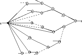
Figure 1. Example of CPT in a fanout-free circuit

Figure 2 shows a circuit with a re-convergent fanout, with two different test vectors. The argument used in conjunction with Figure 1 for finding critical path lines can be used to mark all the critical lines of Figure 2 (shown in both 2-a and 2-b) except the fanout stem. The decision to mark the fanout stem critical depends on the effects of the stem on the gates influenced by this line. In Figure 2-a toggling the value on the fanout stem does not cause the output to change value, while in Figure 2-b the value 0 on the fanout stem causes the output to change from 1 to 0. Therefore the fanout stem in Figure 2-a is not critical, but the test input of Figure 2-b makes the fanout stem to be a critical line.

Figure 2. Critical path tracing, with re-convergent fanout

Considering the examples presented above, there are two key issues in finding faults by critical path tracing. Input lines of a gate whose output is critical can be marked as critical based on the type of the gate and its input and output values. On the other hand, to decide on its stem being critical more than values of fault lines is required. Lines and input values of all gates that fanout branches lead to can participate in the decision to mark a stem as critical. It is not necessary for fanout branches to be critical in order for its stem to be critical. This is another distinguishing feature of fanouts from gates which require their output to be critical if any of their inputs are to become critical.


2.2 CPT METHOD

In the original critical path tracing method [1], primary input values are propagated to all circuit lines. The circuit is traced from output to input for identifying critical lines in a manner similar to what was described in the previous section. In the process of this tracing, when a fanout is encountered, a simulation phase will determine if the effect of changing the value of a fanout stem will be marked as critical. In order to reduce the size of the part of the circuit that is simulated, a partitioning of the circuit is done to simulate only up to the point whose effect on the output is known.

From the above discussion it is clear that critical path tracing by this method requires much forward simulation and backward propagation in an iterative fashion. In addition, partitioning of the circuit into isolated parts with inputs influenced by fanout stem and outputs influencing the primary output is a time consuming process.

Above all, the case mentioned at the end of the previous section in which a fanout stem can be critical even if none of its branches are critical, cannot be handled by the standard CPT method. This is because, the method requires a critical path through branches to reach to a fanout.


3. ONE PASS CRITICAL PATH TRACING

Considering the problems associated with the original critical path tracing algorithm, we have developed a new method that eliminates the need for any partitioning or partial simulation of the circuit. In one pass CPT, simulation is only necessary at the beginning when a test vector is applied. Decision to mark a stem as critical will be based on the information that is passed from gates that are driven by the fanout branches back to the fanout node. In general one pass CPT is centered around the facts that 1) A gate with critical output locally decides on its input lines being critical, and 2) Fanout stems require information from all their branches before they can declare a stem as being critical. Therefore gates, interconnecting lines and fanout nodes must cooperate in providing necessary information to gates and fanout nodes.


3.1 GATE BEHAVIOR

Based on the type and the output value of a gate, a gate makes certain decisions about its input lines. A gate may declare an input line as being critical or it may declare an input as being blocked from becoming critical by another one of its inputs. The expected behavior of a gate is to identify each of its inputs as being critical or being blocked. In a two input AND gate, shown in Figure 3, if only one of the inputs of the gate has a controlling value (Figure 3-a) that input line is critical and the other is blocked, from being critical. If both inputs of a two input gate have controlling values, Figure 3-b, then each input is considered as blocked by the other input. Therefore, both inputs will be refereed to being as blocked. In this case if both inputs change simultaneously, the output value will toggle. As shown in Figure 3-c, if both inputs of a gate have non-controlling values then both inputs are critical, since changing each input will change the output value. The significance of a gate in one pass CPT is only due to its critical and blocked input lines. The notation shown in Figure 4 is a simple notation that eases our analysis of critical path tracing . Critical lines are shown by solid lines, while dotted lines represent blocked lines.


Figure 3. AND gate behavior


Figure 4. Gate notations
a) One critical and one blocked input
b) Two blocked inputs c) Two critical inputs.


3.2 GATE INTERCONNECTION

An interconnection of several gates for critical path tracing can be done by use of a graph using the notation presented in section 3.1. Such a graph will be refereed to as critical path graph (CPG). Figure 5 shows a simple AND-OR circuit and its corresponding CPG.

Figure 5. Critical path graph

The graphs show lines leading to nodes. In this and other graphs shown in this paper, two lines lead to a node, indicating use of two input gates. Lines leading to a node are either Critical or they are Blocked . We will therefore define Kind of line as being CL (critical Line) or BL (Blocked Line). As is Figure 4, solid lines (normal or bold) represent critical lines and dotted lines show blocked lines. Furthermore we define a path as connection of several line segments. A critical path consists of continuos critical lines that lead to a primary output. In Figure 5 bold lines signify CLs that are on a critical path. A blocked path (BP) can be blocked by multiple number of gates. Therefore an n integer appended to the kind of a path signifies the number of gates that block the path from being critical (BPn, n = 1, 2, ...). Path kinds for the example of Figure 5 are shown in Figure 6.

Figure 6. Path kinds

A fanout node will be represented by a filled circle in critical path graphs. Therefore a line can either connect gates or a gate and a fanout. The following paragraphs formalize the definitions of this section.

CPG: Critical Path Graph is a graph formed by replacing logic gates with circles and fanouts with filled circles. In such a graph interconnections are identified by lines according to the following definitions.

Node: A Node represents a gate or a fanout in a CPG.

Line: Lines represents interconnections between gate inputs and outputs as well as fanout edges and stems.

CL or BL: Critical or Blocked lines are those identified by a graph node as being critical or being blocked.

Critical path: A path is critical if all its Line segments are critical and it leads to a primary output.

Blocked path: A path is blocked if it contains at least one blocked line. Blocked path n (BPn) is a BP with n blocked lines.


3.3. FANOUT BEHAVIOR

In addition to gates determining the kind of their input lines, the other decision made in one pass critical path tracing is the decision to mark a fault stem as being critical to not critical. This decision is made by a fanout node and will be based on the types of paths (CP and BPn) associated with fanout branches. The following definition is needed for study of fanout behavior.

Loop: A reconvergent fanout not containing another reconvergent fanout is called a loop. Obviously loop has a convergence and a divergence point.

A loop in a CPG can either be removed or replaced by a critical line, according to the following rules.

Rule a: A loop containing no BLs at the convergence point and at least one continuos path of CLs between convergence and divergence points can be replaced by a CL starting from divergence point (fanout node) and ending in the convergence point (gate).

As an application of this rule consider the circuit of Figure 7 in which the stem at the divergence point directly influences the output of the gate at the convergence point. This direct relationship can more easily be represented by a straight line from stem to the output. For critical values such a loop and a line have equivalent behavior (Figure 7).

Figure 7. Rule a replaces two converging critical paths

Rule b: A loop with only one blocked line at the reconvergence point and at least one continuos path of CLs between convergence and divergence points is removed.

Justification for this rule can be explained in the circuit of Figure 8. Since the AND gate at the output is blocking the propagation of values from gate b to the output of the circuit, and since values at the output of gates a and b both depend on the fanout stem x, therefore changing value of x causes both a and b output to change. This will reverse values at the input of gate c. Instead of output of b being blocked by a, now output of a is being blocked by b. Therefore, values from x do not propagate to the z output. This is represented by a disjoint CPG as shown in Figure 8.

Figure 8. Rule b removes a converging CP and BP

Rule c: A loop with both lines blocked at the convergence point and no other blocked lines is represented by a straight line between divergence and convergence points.

The example of Figure 9 is used for justifying this rule. Since the two inputs of gate c are both 0, it can be said that the two are blocking each other and therefore both can be considered as blocked lines. Changing the value at the stem from 0 to 1 causes both inputs of gate c to change. This represents a direct dependency between the fanout stem x and output of gate c. This direct relationship can be modeled by a CL line from the fanout stem to the output as shown in Figure 9.

Figure 9. Rule c replaces two converging Bps with a CP

Rule d: A loop with at least a blocked line on each path between divergence and convergence points, except if it is covered by Rule c, must be removed.

The above rules are discussed in conjunction with simple circuits with only one loop between a divergence point and a convergence point. In a more complex structure several interlinked loops can exist. These rules can be applied repeatedly from inner loops of complex structure with divergence and convergence points until all loops are removed or replaced. Determining critical lines in a fanout free circuit can be easily done by the methods described in [1]. Using the above rules we can decide whether a stem is critical or not in only one processing pass.

(a)

(b)

Figure 10. Applying Rules a,b, c, and d

An example illustrates application of the above rules to a fanout for finding faults detected by an input vector. Circuit shown in Figure 10-a has reconvergent fanouts with three edges at the divergence point and two convergence points. For input ABCDE=01000 all line values are first calculated. Based on these values and gate characteristics critical and blocked lines will be known, as shown in Figure 10.b. Whether stem B is critical or not will be decided by the application of Rules a, b, and c.
Initially a loop can be observed between the fanout node and gates a, b, and d. Applying Rule c to this loop reduces it to a straight line, and therefore converting the graph of Figure 10-b to that of Figure 11-a. This graph also contains a loop, for the reduction of which Rule a can be applied. The resulting graph is shown in Figure 11-b.
The reduced graph illustrates that the stem is directly connected to the output. We will therefore conclude that stem is critical. Therefore ABCDD=01000 detects six faults in circuit of Figure 10-a including an sa-0 at stem B.

(a)


(b)

Figure 11. Continuing example of Figure 10

(a)

(b)


(c)

Figure 12. A complete example

In another example of our one pass CPT algorithm we will assume a known CPG based on a given circuit and a given test vector. The CPG for this analysis is shown in Figure 12-a. Applying Rule b to loops (4,5) and (15,16) results in removal of these loops. Rule c reduces loop (8,9) to a CL. Figure 12-b shows the CPG after applying Rule a to loop (10) causes the replicate of this loop with a CL from the fanout node to node 10. Applying Rule a to loop (10) is replaced with a CL. Rule b causes the removal of loop (12,13,14,11), which will result in only one CP between the fanout stem and the primary output. This indicates that stem fault will be detected on the Z output (Figure 12-c).


4. VHDL IMPLEMENTATION

The above rules and their application to logic circuits can be easily implemented in a concurrent programming environment. The above discussion facilitates the presentation of VHDL gate models for performing critical path tracing.
After the initial simulation, and after several delta times, all node values will be known. Based on its output values each gate produces CP or BP on its inputs. Primary outputs, being always on a critical path, initiate critical value determination of the output gates. Therefore gate models may observe a CP transaction on their outputs. Such a gate will decide CP or BP on its inputs. This information will eventually be collected and observed at a fanout node. In order to keep track of paths leading to a fanout, each gate collectively send its identification along with the kind information (Critical or Blocked) on its input line signals.
Faults detected are reported by the individual gates and PIs, and POs. Fault detected at a fanout stem will be reported by gates or PIs immediately connected to it. The VHDL implementation of critical path tracing consists of types, resolution function, gate models and utility programs. In this section each of these parts will be described. Before this description, we will make definitions for relating rules of Section 3 to the VHDL coding.


4.1 INFORMATION FIELDS

Interconnecting lines between gates carry information in the forward and backward directions. In the forward direction only logic values are transmitted. In the backward direction information regarding critical, blocked, and the index n number of blocked paths (CP, BPn) are transmitted. The logical values will be referred to as logic, and the information needed for critical path algorithm will be referred to as path_info.


4.2 CRITICAL LEVELS

Path_info of a node whose forward logical value is not known (U) is none. The code value for this state is -3. At the beginning simulation all line path_info is none. After an input vector is applied to the primary inputs, logic values propagate to the outputs changing logic values to '0' or '1', while keeping path_info values to none. The process of determining path_info begins with outputs identifying themselves as critical (CP). CP is a value that is assigned to the path_info and has a code value of 0. Path_info propagate backwards from output towards the inputs of the circuit. On their way, all lines will receive different values of path_info. If an input of a gate is blocking critical path of another input, its path_info becomes BP1 which has a code value of 1. A BPn blocked by another input becomes BPn+1, increasing its code value by 1.

The level of a path_info is determined by its code value. Therefore, CP with level 0 has the lowest level and a BP5 with level 5 has the highest level. Two adjacent levels are those whose codes are consecutive numbers of 0, or above (i.,e., none is not included).

If a line is neither critical nor it is blocking a critical path, it is UNCP and has a code value of negative 2. A similar line, but one that also contains fanout stem information has a code of -1 and will be referred to as UNCP_I.


4.3 LINE TYPE

A line type for containing logical and path information is shown in Figure 13. This is a record named fsim with logic and path_info elements.


	TYPE fsim IS RECORD
		logic : imp;
		path_info : bkt;
	END RECORD;

Figure 13. Node record

The logic element of an fsim record takes values '0', '1', and 'U'. Initially all line logic values are 'U'. Assigning a value '0' or '1' to any of several connecting lines will change the value of all such lines accordingly. The imp resolved type uses the implication resolution function and it is responsible for this behavior.

The path_info element is an array of 4 rows and 20 columns of integers. Path information on each line is included in this array. In each row, the first integer specifies a code value of a path. Therefore a line that is part of a critical path has a 0 value in position (0,0) of the path_info array. The rest of the integers in a row of this array contain gate identifications for all gates that a critical path has gone through. The other three rows contain similar information which will be described in the following sections.

The path_info element of the fsim record is resolved by the backtracing resolution function (bkt). For non fanout nodes, the role of this function is to pass path information from an input of a gate to output of another. For fanout nodes this function will make decisions regarding passing of path information to fanout stems. The details of this function will be described in a later section.

Figure 14. General CPT model structure


4.4 GATE MODELS

A gate model has inputs and outputs of type fsim and INOUT mode. A model is responsible for forward propagation of logic values, and backward (output to input) propagation of path information. A model is also responsible for reporting its inputs and outputs on which faults are being detected. Each gate has a unique identification number passed to it via a generic clause. A single process in the statement part of a gate architecture handles logical and path information generation. In the following discussion we will use a two input NAND gate for demonstrating the behavior of critical path tracing models. A general outline of a gate model is shown in Figure 14.


4.4.1 LOGIC OPERATION

The code for generation of logic value on the output of a gate is shown in Figure 15. After none 'U' values are observed on all gate inputs, a gate uses logic field of its inputs and assigns proper value to the logic field of its output. At this time the gate goes in the backward mode and will only be sensitive to events on the path_info field of its output. When fault values for specific test vector have been reported by the individual gates, gates will again go into forward mode and again become sensitive to events on their inputs. The process of re-initialization which operates after a gate has reported its detected faults is shown in Figure 16.


 ............
 WAIT UNTIL i1.logic /= 'U' AND i2.logic /= 'U';
 in1 := i1.logic;
 in2 := i2.logic;
 out1 := in1 NAND in2;
 o.logic <= out1;
 ..............

Figure 15. Partial code of a gate behavior


 ............
 --- initialization
 i1 <= none_U;
 i2 <= none_U;
 o <= none_U;
 --- wait until all lines in circuit initialized.
 WAIT FOR 10 PS;
 tn := tn + 1;
 ........

Figure 16. Partial code of a gate behavior


4.4.2 GENERATION OF PATH INFORMATION

A gate waits until an event on its output changes path_info field of the output to a value other than none. This happens when a code value greater than -1 is placed on the path_info of an output. The code value of a path_info greater than -1 is an indication that the output is either on a critical (CP), or it on a blocked path (BPn). In this case, based on input logic values, path information for the path_info fields of the inputs will be determined and assigned to the fields of the individual inputs. The code section responsible for this behavior is shown in Figure 17.


 .........
 ELSIF temp_o(1,1) > -1 THEN
 	IF in1 = '0' AND in2 = '1' THEN
		temp_i1 := added_node(temp_o,id);
		temp_i2 := increment_depth(temp_o,id);
 	ELSIF in1 = '1' AND in2 = '0' THEN
		temp_i1 := increment_depth(temp_o,id);
		temp_i2 := added_node(temp_o,id);
 	ELSIF in1 = '0' AND in2 = '0' THEN
		temp_i1 := increment_depth(temp_o,id);
		temp_i2 := temp_i1;
	ELSE
 ..........

Figure 17. Generating path information

This code is reached when an event occurs on the path_info field of the output. At this point, the path_info includes all the path information accumulated in the backward direction into the output of the gate. A path_info on the output may look like the record shown in Figure 18. This illustrates a critical path that has been marked critical by gates 1, 2, and 5.

Figure 18. A path information example

The path_info assigned to the individual inputs is the ouput path_info modified based on input logic values. Assume the record of Figure 18 is the path_info at the output of a NAND gate. In this gate, if in1 logic value is '0' and in2 is '1', in1 is on critical path, and in2 is on a blocked path.

in1 path_info in2 path_info

Figure 19. Path_info for in1, in2 being 0,1

The code of Figure 17 shows that for in1, the added_node function is called to form path_info. This function appends the id number of the present gate to the path_info and keeps the code value of the output the same. The new path_info is assigned to the path_info of in1. For in2 which is a BP (blocked path) the increment_depth is called. This function copies the first row of path_info into the second row, increments the code value (level) of the first row, and appends the id of the present gate to both rows of the path_info. Incrementing CP (code 0) makes it BP1 (code 1) and incrementing BPn makes it BPn+1. Figure 19 shows path_info for in1 and in2.

Assignment of values to path_info of inputs when they are '1' or '0' is done similarly. For in1, in2 being '00' increment_depth procedure is called for both inputs since each input is being blocked by the other input. For in1, in2 being '11' added_node function, which appends the current gate id to the output path_info while preserving the code value of the output, is called for both inputs.


 IF temp_o(1,1) = -1 THEN
	IF in1 = '1' AND in2 = '0' THEN
		temp_i1 := uncp;
		temp_i2 := temp_o;
	ELSIF in1 = '0' AND in2 = '1' THEN
		temp_i1 := temp_o;
		temp_i2 := uncp;
	ELSIF in1 = '0' AND in2 = '0' THEN
		temp_i1 := uncp;
		temp_i2 := uncp;
	ELSE
		temp_i1 := temp_o;
		temp_i2 := temp_o;
 END IF;

Figure 20. Partial code deciding on a non critical fanout

Path information propagates from gate to gate as described in the previous discussion. When a path_info reaches a fanout, the resolution function at the fanout decides the code value at the stem. A CP path_info with code value 0, becomes a CP on the stem. Since the notation of BPn only applies to gates with an input blocking another, and this notation does not appropriately apply to the fanouts. Therefore, we will use UNCP for a fanout stem that is not CP. The BPn information reaching a fanout may still be needed by other fanouts for deciding their critical values. For this reason an UNCP value at a stem will carry such information along. An UNCP with such information will be refereed to as UNCP_I. If an UNCP_I is blocked, it looses its gate information and becomes UNCP. The partial code of Figure 20 shows the behavior of a gate model when UNCP or UNCP_I path information reach its output.


4.5 PATH INFORMATION EXAMPLE

The circuit of Figure 21 shows path information on various lines of an AND-OR circuit. Since gate 1 in this figure is a PO, its output is CP. The path_info placed by this gate on its input contains its id and code value 0 (for CP). Gates 2, 3, 4, and 5 each append their id to the path_info at their output and assign it to their '0' logic value input

s. This happens because value of '01' on inputs of an AND gate makes the '0' input critical.

The lower input of gate 2 is being blocked by the upper input. Therefore, the path information on this gate includes the critical path of its output plus an indication that this path is being blocked once at gate 2. Since the lower input of gate 6 is on a critical path with respect to its own output, therefore, the path_info on this input consists of the path information on the output with gate 6 id appended to its first row. On the other hand, since the lower input of gate 7 is being blocked, blockage level is increased by 1 (changing BP1 to BP2) and the blockage information on the output of this gate is copied to the second row of the input path information.

Figure 21. Path information for a simple AND-OR circuit


4.6 FANOUT RESOLUTION

Although, all interconnecting lines are resolved, resolution of value is only significant at the fanout nodes, and that is only important when processing path information in the backward direction. The resolution function for this purpose is called backtracing which will be discussed here.

Drivers of the backtracing resolution function are path_info that reach a fanout from various gates. The resolution function makes a copy of all its drivers in a temporary buffer and starts processing and making modifications to this buffer using rules a, b, c of Section 3.


 FUNCTION backtracing (paths : int_4by20_vector) RETURN int_4by20 IS
	VARIABLE temp1, temp2 : int_4by20_vector(paths'RANGE);
	VARIABLE depth, util1 : INTEGER := 0;
	VARIABLE util2, connection : BOOLEAN := false;
	VARIABLE num : INTEGER := INTEGER'HIGH;
	VARIABLE rejector : int_4by20 := rjct;
	VARIABLE constructed, agent : int_4by20 := none;
	VARIABLE select1, select2 : INTEGER := -1;

Figure 22. Resolution function declarative part

Initially the resolution function (the declarative part of which is shown in Figure 22) searches for a path record which has the highest code value of all the other drivers. The highest code value corresponds to a path with most number of blockages. This path being blocked the most, represents part of an innermost loop. The part of the resolution function searching for the deepest BPn is shown in Figure 23.


 FOR i IN paths'RANGE LOOP -------- deepest path will be found.
	IF depth < temp1(i)(1,1) THEN
		depth := temp1(i)(1,1);
	END IF;
 END LOOP; 

Figure 23. Partial code of the resolution function, finding deepest path

In the discussion that follows, CP and BP definitions of Section 3.2 will be used. The following points from the definitions need to be elaborated upon. The level of a CP is always 0. A BPn is a blocked path with n number of blockages, this refers to a path through several gates with n gates blocking it from being critical. The number n is the level of a BP and this number is at least 1. The deepest BPn is one with the highest level (n). Decreasing the level of a BPn results in BPn-1. Decreasing the level of a BP1 results in a CP because the level of CP is 0.


......................
 IF depth > 0 THEN ------------- construct and reject 
    FOR i IN depth DOWNTO 1 LOOP 
       -- path with i depth will be constructed.
       FOR j IN paths'RANGE LOOP
          IF temp1(j)(1,1) = i THEN
 	     FOR l IN j + 1 TO (paths'LENGTH - 1) LOOP
                IF temp1(l)(1,1) = i THEN
 		   replace_check (
 		   temp1(j), temp1(l), constructed, connection);
 	           IF connection THEN
 		      temp1(j) := constructed;
 		      temp1(l) := none;
 	           END IF;
 		END IF; 
 	     END LOOP;
          END IF;
       END LOOP;
 	
       FOR j IN paths'RANGE LOOP 
          ---- path with i-1 depth is rejected
          IF temp1(j)(1,1) = i THEN -- by path with i depth.
 	     FOR l IN paths'RANGE LOOP
 	        IF temp1(l)(1,1) = (i - 1) THEN
 		   remove_check (
 		   temp1(j), temp1(l), constructed, connection);
 		   IF connection THEN
 		      temp1(l) := constructed;
 		   END IF;
 		END IF;
 	     END LOOP;
 	  END IF;
       END LOOP;
    END LOOP;
 END IF; 
 ........

Figure 24. Partial code for the execution of rules a and c

The partial code shown in Figure 24 becomes activate when at least a BPn is found on one of the edges of the fanout stem. In this case, starting from the path information with the deepest BPn, the temporary buffer of all drivers is searched for another path information with an equal BPn (see Figure 24). If such a driver is found then the replace_check function determines if the two path_info have a common node at the convergence point. If so, using rules a or c these path_info will be replaced by BPn or BPn-1 in the temporary buffer. If rule a is used, the two paths will be replaced by a path with same level, while application of rule c causes the replacement path level to become n-1.

After application of rules a and c, as above, the resolution function searches the temporary buffer for remaining BPn path_info that have not been replaced by BPn-1. In this case, if a BPn-1 is found that has a common node at the convergence point with the BPn under consideration, then the two path_info will be removed from the temporary buffer. This removal process is done by performing rules b and d, which are checked by the remove_1_check function.

The above processes, in which rules a, c and b, d are applied, will be repeated for all path_info from highest to the lowest blocked level (BP1). When this is done, if the resulting path_info in the temporary buffer has level 0 (CP), then the fanout stem is critical, otherwise the fanout stem will be declared as being un-critical (UNCP_I).


5. USE ENVIRONMENT

The critical path analysis models can be used for non-deterministic test generation of for fault simulation. Because the netlist is a standard VHDL instantiation list, the same netlist can be used for other test activities such as VHDL based test generation or fault list generation [8,9]. In this section we will demonstrate the use of our models for fault simulation through the use of an example.


 ......
 PI3 : pi GENERIC MAP(3)
 PORT MAP(S(3));
 PI4 : pi GENERIC MAP(4)
 PORT MAP(S(4));
 G8 : or2 GENERIC MAP(9)
 PORT MAP(S(6),S(4),S(7));
 G9 : or2 GENERIC MAP(10)
 PORT MAP(S(9),S(8),S(10));
 G10 : not1 GENERIC MAP(11) 
 PORT MAP(S(10),S(11));
 ......

Figure 25. Instantiation list

A full-adder, the partial gate list of which is shown in Figure 25, constitutes the complete VHDL description for fault simulation for the purpose of test grading. The components of this circuit are bound to primary input, simple logic gates, and primary output CPT models. The nodes in this description are resolved and of the fsim type. The PI models are responsible for reading their corresponding test vectors from a test file and applying them to their outputs. Gate models behave according to the one pass CPT method as described in Section 4.


 TEST:GATE(ID) *****DETECTED SSF***** ]
 ...... ..............................
 1:OR2 ( 9) [I1:sa_0; I2:none; O1:sa_0 ]
 1:OR2 (10) [I1:none; I2:none; O1:sa_0 ]
 1:NOT (11) [I :sa_0; O :sa_1 ]
 1: PO (12) [PO:sa_1; ]
 2: PI ( 1) [PI:sa_1; ]
 2: PI ( 4) [PI:sa_1; ]
 ........................................ 

Figure 26. Partial Detected Fault Report

Faults detected by test vectors applied by the PIs will be reported by the individual gate models. Figure 26 shows a partial list of detected faults reported for the full-adder of Figure 25. This list shows a test vector and gates on which faults are detected. Faults on a line connecting a gate output to another gate input will be reported by both gates.


6. CONCLUSIONS

In this paper, we have presented a new method of critical path tracing for fault simulation. This method is called one-pass CPT and it performs critical path tracing in only one output-to-input pass. We avoid circuit partitioning and incremental simulation of the circuit. Rule c detects critical stems that are not detected by the present CPT methods. We have implemented the one-pass CPT in VHDL. This language is specially appropriate because of its ability to model concurrent processes. We have developed other VHDL based test related tools such as test generation and fault collapsing. The combination of such models used in a test environment can provide necessary test tools for hardware designers using the VHDL language based tools in their designs. The models presented here suggest a new test methodology as well as new application for the VHDL language. Although, results have been verified with use of conventional methods, performance comparison is not relevant at this point.


REFERENCES:

[1] M. Abramovici, P. R. Menon and D. T. Miller. "Critical Path Tracing - An Alternative to Fault Simulation", IEEE Design and test, Feb. 1984, pp. 83-92.

[2] T. Ramakrishman and L. Kinney. "Extension of Critical Path Tracing" Design Automation Conference, 1990, pp. 720-723

[3] K. J. Antereich and M. H. Schulz. "Accelerated Fault Simulation and Fault Grading in Combinational Circuits", Transaction on Computer Aided Design, 1987, pp. 704-712.

[4] S. K. Jain and V. D. Agrawal, "STAFAN : An Alternative to Fault Simulation", Design Automation Conference, 1984, pp. 475-480

[5] V. D. Agrawal, "Sampling Technique for Determining Fault Converge in LSI circuits", J. Digital sys., vol. V, no. 3, 1981, pp. 189-202.

[6] Z. Navabi, N. Cooray and R. Liyanage. "Using VHDL in parallel fault simulation" proc. scs., International Conference on Simulation in Engineering Education. January 17-20, 1993,Vol . C-25, no. 3.pp.198-203.

[7] Z. Navabi, VHDL: Analysis and Modeling of Digital Systems, McGraw Hill, New York, 1993.

[8] Z.Navabi, F.Khani, "VHDL Structural Models for the Implementation of Path Sensitization Test Generation" ICEHDL WMC 1995, Submited.

[9] Z. Navabi, M. Shadfar, "VHDL Modeling for Equivalence Fault Collapsing", Proc. VHDL International Users' Forum. May 1-4, 1994.