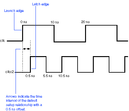
In the fir_filter design, the 0.5 ns offset you specified for the clockb clock settings causes the Timing Analyzer to report that timing requirements were not met. This condition was intentionally created for this tutorial in order to demonstrate how the Multicycle timing assignment affects the default setup relationship.
By default, the Timing Analyzer uses the most restrictive setup relationship when analyzing paths between registers that are clocked by different clocks. The Timing Analyzer verifies that the data is present at the destination register in time to be properly latched.
In designs with multiple clocks, for every latch edge on the destination clock, the launching edge on the source register determines the delay requirement for the path. In the fir_filter design, for every latch edge of the destination register, the Timing Analyzer finds the nearest launch edge that precedes each capture edge. The smallest difference determines the maximum delay requirement.
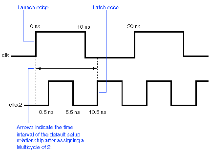
You can use the Multicycle timing assignment to specify a path that requires more than one clock cycle to propagate. Assigning a Multicycle of 2 to all registers clocked by clkx2 allows you to override the default setup relationship and delay the latch edge by one clock cycle, thus achieving the specified timing requirements.
|