With the Selection and Smart Drawing Tool, double-click the default pin_name pin name of the first input pin symbol you entered.
To rename the pin_name default block name, type clkx2 and press Enter.
| You can also specify the pin name by double-clicking the pin, and then specifying the pin name in the General tab of the Pin Properties dialog box. |
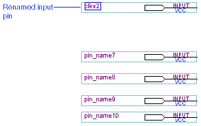
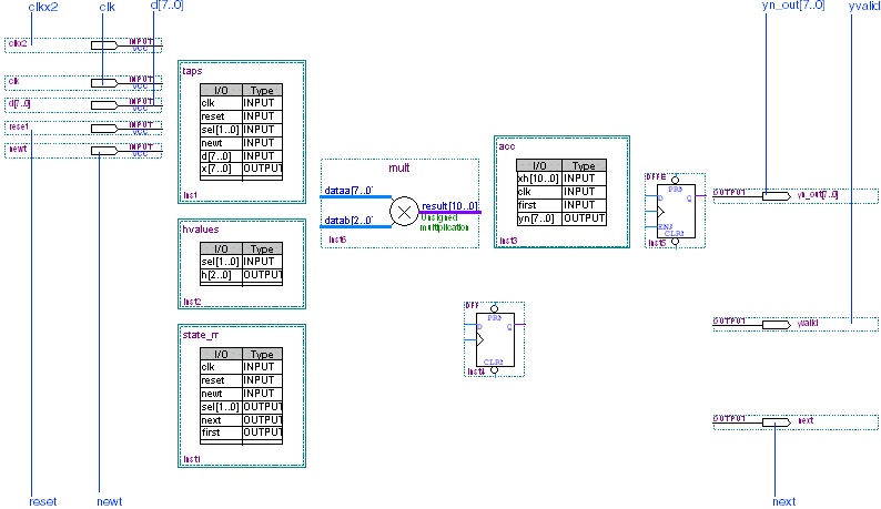
Repeat steps 1 and 2 to rename each of the pins with the following names:
| Pin Type: | Rename As: | Description: |
INPUT |
clkx2 (already entered) |
Derived clock for the FIR filter. |
INPUT |
clk |
Base clock for the FIR filter. |
INPUT |
d[7..0] |
Data input to the FIR filter. |
INPUT |
reset |
Reset signal for the FIR filter. |
INPUT |
newt |
Input signal that loads the data input d[7..0]
into the taps function. |
OUTPUT |
yn_out[7..0] |
The FIR filter output data. |
OUTPUT |
yvalid |
Indicates that the yn[7..0] filter output
of the acc function is valid. |
OUTPUT |
next |
Indicates that the FIR filter is ready for the next 8-bit data input. |
Move the INPUT and OUTPUT pin symbols so they line up with the appropriate symbols or blocks, as shown in the following illustration:
Choose Save (File menu).