For Printing Purposes Only! |
|
Click the Print icon to print this Module. Click the Done or Previous button when finished. |
Timing Analysis Module |
With the Quartus II Timing Analyzer, you can analyze the timing performance of all logic in your design. You can trace signal paths and locate them in the Floorplan Editor, determining critical speed paths that limit the design's performance.
The Quartus II Timing Analyzer runs automatically at the end of the compilation process, or you can run the Timing Analyzer separately after first-time project compilation. When timing analysis is complete, timing information is reported in the Timing Analyses folder of the Compilation Report.

The Timing Analysis tutorial module guides you through the steps necessary to view the timing analysis results in the Compilation Report window, specify timing requirements, perform multiclock timing analysis, and assign a multicycle path.
|
If you have not already sequentially completed the Design Entry and Compilation tutorial modules, you must first open and compile the timing analysis project before you can begin working in the Timing Analysis tutorial module.
To open the timing analysis project, follow these steps:
Choose Open Project (File menu). The Open Project dialog box appears.
In the \qdesigns\fir_filter\timing subdirectory, select the Altera-provided timing_fir_filter.quartus project file in the Files list.
Click Open.
Choose Start Compilation (Processing menu). The Compiler compiles the design.
When you receive a message indicating that compilation was successful, click OK.
|
After you compile a design, you can view the timing analysis results in the Compilation Report. By default, the Timing Analyzer reports the maximum frequency (fMAX) of every register, the worst-case register-to-register delays, the input setup (tSU) and input hold (tH) times of every input register, the clock-to-output (tCO) delays of every output register, and the pin-to-pin (tPD) delays between all pins. In addition, you can customize the timing analysis by specifying timing requirements and other options.
|
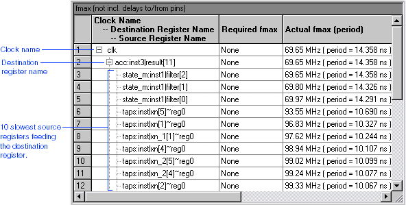
The fmax section of the Compilation Report shows the frequency requirements and worst-case speed performance of your design.
To open the fmax section of the Compilation Report, follow these steps:
If necessary, to open the Compilation Report, choose Compilation Report (Processing menu).
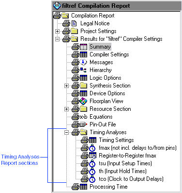
In the left pane of the Compilation Report window, click the + icon to expand the Timing Analyses folder.
Under the Timing Analyses folder, select the fmax section. The fMAX information appears in a table.
To expand the list and display the destination registers associated with the clock, click the + icon next to the clk clock name. By default, the list expands to show the 10 slowest destination registers.
| You can go to "Specifying Timing Analysis Reporting Restrictions" in Quartus II Help for information about customizing timing analysis reporting. | |
|
To list the fMAX timing paths, follow these steps:
To expand the list and display the source registers feeding a destination register, click the + icon to expand the first destination register name in the fmax section. By default, the list expands to show the 10 slowest source registers.
![]()
Select the first source register name in the list.
Choose List Paths (right button pop-up menu). The delay paths for the source register, including intermediate delay paths, appear as messages in the System tab of the Messages window.
In the Messages window, click the + icon to expand the Clock <name> has Internal fmax of message. The Longest register to register delay, Smallest Clock skew, Micro clock to output delay, and Micro setup delay messages are displayed.
![]()
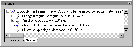
Click the + icon to expand the Longest register to register delay message. The intermediate time increments used to calculate the timing path delay are displayed.
|
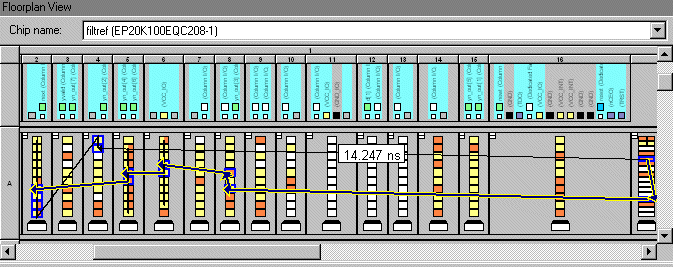
To locate the source of a timing path message in the Last Compilation floorplan, follow these steps:
In the Messages window, select the Longest register to register message.
Choose Locate (right button pop-up menu). The data path is highlighted in the floorplan, and the total timing path delay appears alongside the path.
![]()
|
The tsu section of the Compilation Report displays the actual setup time tSU for the input pins that feed the data or clock enable inputs to the destination register.
To open the tsu section of the Compilation Report, follow these steps:
In the left pane of the Compilation Report window, click the + icon to expand the Timing Analyses folder.
Under the Timing Analyses folder, select the tsu section. The input setup time information is displayed in a table.
To expand the list and display the register and clock name(s) associated with the data pin, click the + icon.
When you are finished viewing the paths, choose Close (File menu).
| You can also view other sections in the Compilation Report by modifying the procedures above. Specific steps for viewing all timing analysis results are described in "Viewing Timing Analysis Results in the Report Window" in Quartus II Help. | |
|
Timing requirements allow you to specify the desired speed performance for the entire project, for specific design entities, or for individual nodes and pins. For example, you can specify project-wide timing requirements for the setup time (tSU), hold time (tH), clock-to-output delay (tCO), pin-to-pin delays (tPD), and maximum frequency (fMAX).
In addition, you can override the default timing requirements on specific portions of the design by making individual timing assignments. You can also assign other individual timing assignments to cut timing paths, add external input or output delays, and invert clocks to further optimize your design. If you specify both individual and project-wide timing requirements, the Compiler uses the most stringent requirements.
You can specify timing requirements for the entire project with the Timing Settings command (Assignments menu), or you can specify timing requirements for individual entities, nodes, and pins with the Assignment Organizer command (Assignments menu). If you specify either project-wide or individual timing requirements, the Fitter optimizes the placement of logic in the device in order to meet your timing goals when you use timing-driven compilation.
| The following procedures explain how to specify timing requirements and other timing analysis settings using menu commands and dialog boxes. However, you can also easily specify timing requirements and other timing analysis settings by following the steps in the Timing Wizard (Assignments menu). |
|
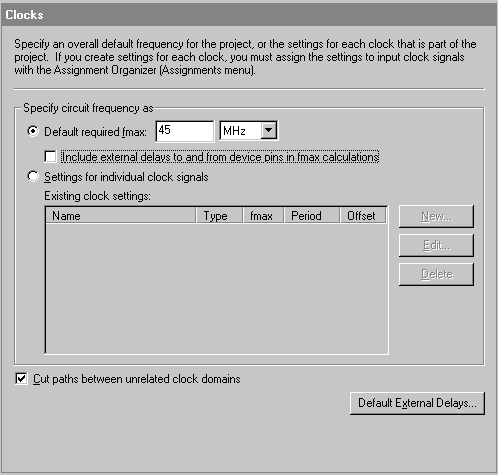
You can specify a default fMAX for an entire project, or you can specify a required fMAX for selected portions of the project.
To specify the default required fMAX, follow these steps:
Choose Timing Settings (Assignments menu). The Timing Settings page of the Settings dialog box appears.
In the Category list, select Clocks under Timing Settings. The Clocks page appears.
Under Specify circuit frequency as, Make sure Default required fmax is selected.
In the Default required fmax box, type 45 and select MHz in the list. The Fitter will now optimize the placement of logic in the device in order to meet this timing goal, and the Timing Analyzer reports any signals that do not acheieve the fMAX requirement during compilation.
![]()
| You can override this default required fMAX for individual clocks in your design by creating clock settings and assigning them to individual clock signals in your design. This procedure is described later in this tutorial. |
|
You can direct the Timing Analyzer to ignore specific signal paths by cutting them from the timing analysis. You can turn on options in the Other Requirements & Options page (Settings dialog box) to cut all instances of specific categories of paths, or you can cut specific paths on a node-by-node basis with the Cut Timing Path assignment in the Assignment Organizer (Assignments menu).
To globally cut off feedback from I/O pins, follow these steps:
In the Settings dialog box, select Other Requirements & Options under Timing Settings. The Other Requirements & Options page appears.
Make sure Cut off feedback from I/O pins is turned on. The Timing Analyzer will now ignore all signal feedback from within the device.
Click OK.
|
The Quartus II Timing Analyzer automatically performs single-clock frequency analysis as part of compilation. However, the Timing Analyzer can also perform timing analysis on designs that use complex timing assignments, such as designs with multiple clocks.
To perform an accurate multiclock analysis, you must first define the relationship between all clocks in the design. To define this relationship, you must specify which signals function as the absolute clocks (not dependent on other clocks) and the derived clocks (dependent on other clocks) in the design. In the Quartus II software, you define the behavior and requirements of clocks by creating clock settings. Then, you assign these settings to the clock signals in the design.
|
To create absolute clock settings, follow these steps:
Choose Timing Settings (Assignments menu). The Timing Settings page of the Settings dialog box appears.
In the Category list, select Clocks under Timing Settings. The Clocks page appears.
Under Specify circuit frequency as, select Settings for individual clock signals.
Click New. The New Clock Settings dialog box appears.
In the Clock settings name box, type clocka as the name for the new group of clock settings.
To specify that these clock settings are for an absolute clock, under Relationship to other clock settings, make sure Independent of other clock settings is selected.
To specify the required fMAX of the absolute clock, in the Required fmax box, type 50 and select MHz in the list.
![]()
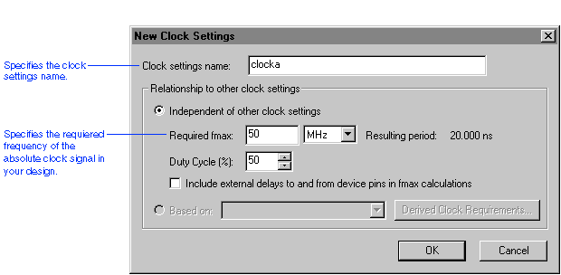
Click OK. The clocka settings appear in the Existing clock settings list.
|
To create derived clock settings, follow these steps:
In the Clocks page, click New. The New Clock Settings dialog box appears.
In the Clock settings name box, type clockb.
Under Relationship to other clock settings, select Based on and select clocka in the list.
To specify timing requirements for the derived clock, click Derived Clock Requirements. The Derived Clock Requirements dialog box appears.
To specify that the derived clock is a multiple of two of the absolute clock, select 2 in the Multiply base absolute clock fmax by list.
To specify that the derived clock is offset from the absolute clock, type 0.5 in the Offset from base absolute clock fmax box and select ns in the list.
![]()
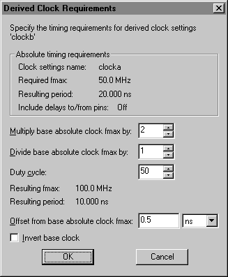
Click OK.
In the New Clock Settings dialog box, click OK to add the clockb clock settings to the Existing clock settings list.
In the Settings dialog box, click OK.
|
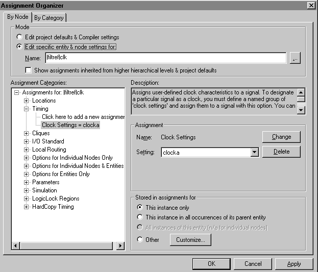
Once you have defined an absolute or derived clock setting, you must assign the setting to the appropriate clock signal(s) in the design. In the Quartus II software, you can use the Assignment Organizer command (Assignments menu) to create, delete, edit, and view the assignments in the project.
To assign the clocka settings to the clk pin, follow these steps:
Choose Assignment Organizer (Assignments menu). The By Node tab of the Assignment Organizer dialog box appears automatically.
Under Mode, select Edit specific entity and node settings for.
![]()
Under Mode, click Browse (...) next to the Name box. The Node Finder dialog box appears.
To find the clock signal name to which you want to assign the clock settings, in the Node Finder dialog box, select Pins: all in the Filter list and then click Start.
![]()
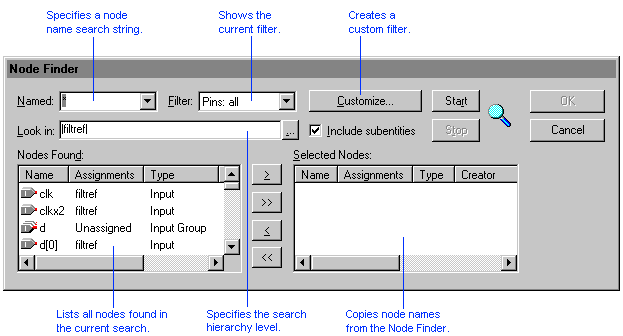
In the Nodes Found list, double-click the clk pin name.
To copy the clk pin name to the Assignment Organizer dialog box and close the Node Finder dialog box, click OK.
|
To continue assigning the clock settings to a pin, follow these steps:
In the Assignment Organizer dialog box, click the + icon to expand Timing in the Assignment Categories list.
Click the Click here to add a new assignment text.
Under Assignment, in the Name list, make sure Clock Settings is selected.
To identify the clock settings that should be assigned to the pin, make sure clocka is selected in the Setting list.
Click Add. The new assignment appears in the Assignment Categories list.
![]()
Under Mode, click Browse (...) next to the Name box. The Node Finder dialog box appears.
To remove the clk pin name from the Selected Nodes list, click Remove all nodes (<<).
To find the clkx2 pin to which you want to assign clock settings, in the Node Finder dialog box, click Start.
In the Nodes Found list, double-click the clkx2 pin name.
To copy the clkx2 pin name to the Assignment Organizer dialog box and close the Node Finder dialog box, click OK.
Repeat steps 7 through 11 to assign the clockb settings to the clkx2
pin.
In the Assignment Organizer dialog box, click OK.
| You can also specify many other types of individual timing assignments. You can go to "Making Individual Timing Assignments" in Quartus II Help for more information on available timing assignments. | |
|
To rerun timing analysis:
Choose Start > Start Timing Analysis (Processing menu).
When the Quartus II software asks whether you want to recompile before starting timing analysis, click No. The timing analysis runs without recompiling the design.
| The Quartus II software asks you if you want to recompile at this point because specifying timing requirements affects fitting when you are using timing-driven compilation. However, for this tutorial, recompilation is not necessary. |
When the Quartus II software informs you that the timing analysis was successful, click OK. Note that a message appears in the Messages window indicating that timing requirements were not met.
|
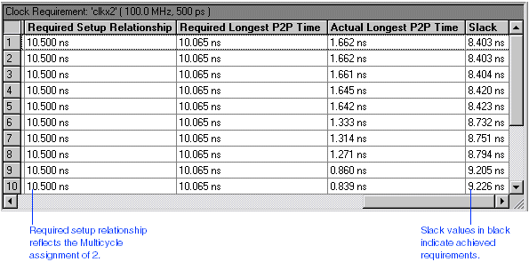
In designs that use complex timing assignments, the Timing Analyzer generates a Clock Requirement section, rather than an fmax section, for each clock signal you designate in the design. The Clock Requirement section reports the speed performance as a "slack" value. Slack is the margin by which a timing requirement was achieved or not achieved. A positive slack value, displayed in black, indicates that the requirement was achieved. A negative slack value, displayed in red, indicates that the requirement was not achieved.
To view the Clock Requirement section for the clkx2 signal, follow these steps:
In the left pane of the Compilation Report window, click the + icon to expand the Timing Analyses folder.
Under the Timing Analyses folder, select the Clock Requirement section for the clkx2 signal. The timing analysis information is displayed in a multi-column table. If necessary, drag the resizing tool to resize columns in the table.
![]()
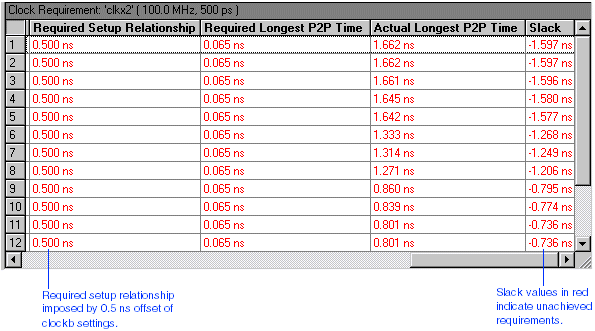
The Clock Requirement section for the clkx2 signal displays slack values in red, indicating that the specified fMAX requirement was not achieved along the path. The following section describes how to specify a multicycle path that corrects this condition.
|
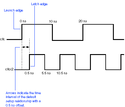
In the fir_filter design, the 0.5 ns offset you specified for the clockb clock settings causes the Timing Analyzer to report that timing requirements were not met. This condition was intentionally created for this tutorial in order to demonstrate how the Multicycle timing assignment affects the default setup relationship.
By default, the Timing Analyzer uses the most restrictive setup relationship when analyzing paths between registers that are clocked by different clocks. The Timing Analyzer verifies that the data is present at the destination register in time to be properly latched.
In designs with multiple clocks, for every latch edge on the destination clock, the launching edge on the source register determines the delay requirement for the path. In the fir_filter design, for every latch edge of the destination register, the Timing Analyzer finds the nearest launch edge that precedes each capture edge. The smallest difference determines the maximum delay requirement.
![]()
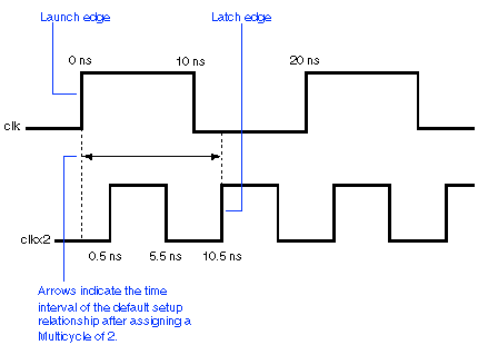
You can use the Multicycle timing assignment to specify a path that requires more than one clock cycle to propagate. Assigning a Multicycle of 2 to all registers clocked by clkx2 allows you to override the default setup relationship and delay the latch edge by one clock cycle, thus achieving the specified timing requirements.
![]()
|
You can make individual timing assignments to a single node or to a path between a source and destination point. When you make a point-to-point assignment to the path between two clock pins, the assignment is automatically applied to all register-to-register paths between the two clocks. To add the Multicycle assignment to all register-to-register paths between the clk and clkx2 pins, follow these steps:
To open to the filtref.bdf block diagram, choose Open (File menu). The Open dialog box appears.
In the Files of type list, select Device Design Files.
In the Files list, select filtref.bdf.
Click Open.
In the filtref.bdf block diagram, select the clkx2 input pin.
Choose Assignment Organizer (right button pop-up menu). The Assignment Organizer dialog box appears, with the Edit specific entity & node settings for option selected, and with the hierarchical path name of the clkx2 pin shown in the Name box.
In the Assignment Categories list, click the + icon to expand Timing.
Click the Click here to add new assignment text.
Under Assignment, select Multicycle in the Name list.
To specify a multicycle path that requires two clock cycles to propagate, in the Setting box, type 2.
To specify the source point for a point-to-point assignment, in the Fed by box, type clk or click Browse (...) to select the pin name with the Node Finder dialog box.
Click Add. The assignment appears in the Assignment Categories list.
Click OK.
|
To rerun timing analysis:
Choose Start > Start Timing Analysis (Processing menu).
When the Quartus II software asks whether you want to recompile before starting timing analysis, click No. The timing analysis runs without recompiling the design.
When the Quartus II software informs you that the timing analysis was successful, click OK. Note that a message appears in the Messages window indicating that all timing requirements were met.
|
To view the timing analysis results to determine how setting the Multicycle assignment affected timing requirements, follow these steps:
In the left pane of the Compilation Report window, click the + icon to expand the Timing Analyses folder.
Under the Timing Analyses folder, select the Clock Requirement section for the clkx2 signal. The Clock Requirement section displays all slack values in black, indicating that all timing requirements were achieved after overriding the default setup relationship with the Multicycle assignment.
![]()
|