For Printing Purposes Only! |
|
Click the Print icon to print this Module. Click the Done or Previous button when finished. |
Design Entry Module |
In the Quartus II software, a "project" consists of the complete set of design files, assignment files, simulation files, system settings, and hierarchy information for a design. The Design Entry tutorial module guides you through the steps needed to create the fir_filter tutorial project, and then explains how to create a top-level Block Design File (.bdf) that contains blocks representing the lower-level design files. Next, you create the lower-level Verilog Design Files (.v) that these blocks represent. You complete the Design Entry module by creating a custom megafunction variation that is instantiated by one of the lower-level design files. The project you create in this module demonstrates top-down design methodology.
|
The Quartus II software offers a New Project wizard to help you create a new project. You can subsequently edit these project settings using menu commands and dialog boxes. To create a new project using the New Project Wizard, follow these steps:
Choose New Project Wizard (File menu). The New Project Wizard appears. The first time you open the New Project Wizard, it may display the Introduction page; you can click Next to proceed to the first page of the wizard.
Type the directory name in the working directory box, or select the directory with Browse (...). For this example, type d:\qdesigns\fir_filter or browse to select it.
Type a name for the project in the project name box. For this example, type fir_filter.
Type filtref as the name of the top-level design entity of the project in the top-level design entity box.
| By default, the project name you enter appears as the name of the top-level design entity. However, you can use a different top-level design entity name, as this step directs you to do. |
![]()

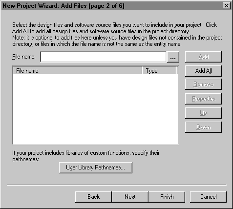
Click Next. The Add Files page of the New Project Wizard appears. Because fir_filter is a new project, there are no files to add to this project yet. If design files already existed for this project, you could use Browse (...) to select the files, and then click Add to add them to the project.
![]()
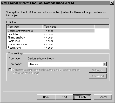
Click Next. The EDA Tool Settings page of the New Project wizard appears. This page allows you to specify options for other EDA tools for use with this project. Since this project does not use other EDA tools, make sure that None is specified in the Tool name column for each tool type.
![]()
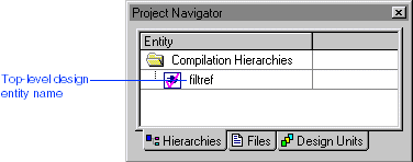
To accept the default settings for the remaining wizard prompts and create the project, click Finish. The project is now created. The top-level design entity name appears in the Hierarchies tab of the Project Navigator window.
![]()
|
This section describes how to create a block diagram as the top-level design entity in the project. You begin by creating the top-level design entity, filtref.bdf.
| At several stages in this tutorial, you can significantly reduce the time required to complete the tutorial by copying Altera-provided design files, rather than creating those files from scratch. If you are already familiar with design entry using the Quartus II Block Editor, and you want to use the Altera-provided design files, go to Copying Altera-Provided Design Files for more information. |
|
In this step you create a new BDF called filtref.bdf. This file is the top-level design entity of the fir_filter project.
To create a new BDF, follow these steps:
Choose New (File menu). The Device Design Files tab of the New dialog box appears automatically.
Select Block Diagram/Schematic File.
Click OK. A new Block Editor window opens.
Choose Save As (File menu). The Save As dialog box appears.
Select the folder where you want to save the BDF. The Save As dialog box should automatically display the project directory name, d:\qdesigns\fir_filter, as the directory for saving the file.
In the File name box, type filtref as the name, if necessary.
Make sure Add file to current project is turned on.
To save the file and add it to the project, click Save.
|
Follow these steps to create the taps block in the filtref.bdf file:
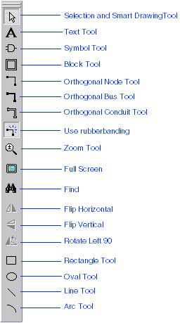
In the Block Editor window, click the Block Tool button ![]() on the toolbar.
on the toolbar.
![]()
Click a blank space in the Block Editor and drag the Block Tool pointer until the block is the size you want.
![]()
| You can use the Undo and Redo commands (Edit menu) to make corrections, if necessary. |
Click the Selection and Smart Drawing Tool button ![]() on the toolbar.
on the toolbar.
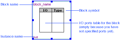
With the Selection and Smart Drawing Tool, double-click the block_name default block name.
To rename the block_name default block name, type taps and press Enter.
| You can also specify the block name by double-clicking the block, and then specifying the block name in the General tab of the Block Properties dialog box. |
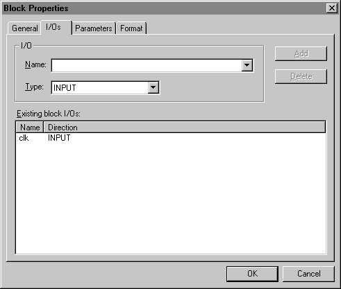
With the Selection and Smart Drawing Tool, double-click in the I/O column of the taps block. The I/Os tab of the Block Properties dialog box appears automatically.
Under I/O, type clk in the Name box as the first
port name, and in the Type list, select INPUT.
Click Add. The clk port name appears in the Existing
block I/Os list.
![]()
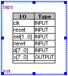
Repeat steps 7 and 8 to enter each of the port names shown in the following table:
| You can also type in all of the input port names at once, separating each name by a comma, and then click Add. |
| Name: | Type: |
clk (already entered) |
INPUT |
reset |
INPUT |
sel[1..0] |
INPUT |
newt |
INPUT |
d[7..0] |
INPUT |
x[7..0] |
OUTPUT |
Click OK. You have now specified the input and output ports of the taps block.
Select the taps block.
Choose AutoFit (right button pop-up menu). This command resizes the border of the taps block to fit proportionally around the I/O ports table, and ensures that all data about the block is visible.

|
Follow these steps to create the state_m, hvalues, and acc blocks in the filtref.bdf file:
Repeat steps 1-12 described
in Step 2: Create the taps Block to create the state_m, hvalues,
and acc blocks with the ports listed in the following tables:
Specify these ports for the state_m block:
| Name: | Type: |
clk |
INPUT |
reset |
INPUT |
newt |
INPUT |
sel[1..0] |
OUTPUT |
next |
OUTPUT |
first |
OUTPUT |
Specify these ports for the hvalues block:
| Name: | Type: |
sel[1..0] |
INPUT |
h[2..0] |
OUTPUT |
Specify these ports for the acc block:
| Name: | Type: |
xh[10..0] |
INPUT |
clk |
INPUT |
first |
INPUT |
yn[7..0] |
OUTPUT |
Choose Save (File menu).
|
A BDF can contain both block symbols, like those you have already created in this tutorial, and "ordinary" schematic symbols. The Quartus II software provides symbols for a variety of logic functions—including primitives, Library of Parameterized Modules (LPM) functions, and other megafunctions—that you can use in the Block Editor.
Follow these steps to enter a DFF (D flipflop) symbol in the filtref.bdf file:
Double-click any empty space in the Block Editor window. The Symbol dialog box appears.
In the Libraries list, click the + icon to expand the d:\quartus\libraries folder. Similarly, expand the primitives folder, and then expand the storage folder.
In the storage folder, select the dff primitive. A preview of the new symbol appears in the Symbol dialog box.
![]()

As shortcut for steps 2 and 3, you can simply type dff in the Name box. |
Click OK. An outline of the DFF symbol is now attached to the pointer.
Click the pointer at the desired location in the Block Editor window to insert the DFF symbol into the design file.
Repeat steps 1 through 5 to enter a DFFE symbol in the filtref.bdf file.
|
The next symbol you need to enter is a multiplier that is a variation of the lpm_mult megafunction. You can use the MegaWizard™ Plug-In Manager to enter this symbol. The MegaWizard Plug-In Manager allows you to create (or modify) design files that contain custom variations of megafunctions. These custom megafunction variations are based on Altera-provided megafunctions, including Library of Parameterized Modules (LPM) functions. The MegaWizard Plug-In Manager runs a wizard that helps you specify options for customization easily. The wizard prompts you about the values you want to set for parameters and which optional ports you want to use. Once the wizard generates the multiplier variation, you can instantiate it in the design file.
To enter a mult symbol generated by the MegaWizard Plug-In Manager, follow these steps:
Double-click an empty space in the Block Editor window. The Symbol dialog box appears automatically.
In the Symbol dialog box, click MegaWizard Plug-In Manager. The first page of the MegaWizard Plug-In Manager appears.
![]()
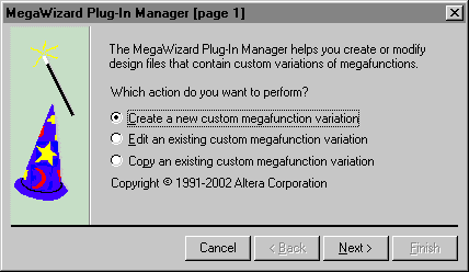
In the first page of the MegaWizard Plug-In Manager, make sure Create a new custom megafunction variation is selected and click Next.
Under Which megafunction would you like to customize?, click the + icon to expand the arithmetic folder, and then select LPM_MULT.
Specify the following responses to the remaining wizard prompts:
| Wizard Prompt: | Response: |
| Which device family will you be using? | APEX20KE |
| Which type of output file do you want to create? | Verilog HDL |
| What name do you want for the output file? | d:\qdesigns\fir_filter\mult.v |
| How wide should the 'dataa' input bus be? | 8 |
| How wide should the 'datab' input bus be? | 3 |
To accept the defaults for the remaining questions and generate the symbol, click Finish. A preview of the new symbol appears in the Symbol dialog box.
Click OK. An outline of the mult symbol is attached
to the pointer.
To place the symbol, click the location you want the mult symbol to appear in the Block Editor window.
Choose Save (File menu).
|
In this step, you arrange the blocks, symbols, and megafunction in the Block Editor window in preparation for making connections.
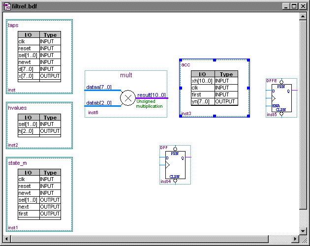
| Click the Selection and Smart Drawing Tool button on the toolbar or press Esc to activate the Selection and Smart Drawing Tool, and then drag the blocks, primitives, and megafunction to arrange them as shown in the following illustration:
|
|
You can change the Block Editor display options, as needed. To change the Block Editor display options, follow these steps:
Choose Options (Tools menu). The Options dialog box is displayed.
In the Category list, under Block/Symbol Editor, select General.
In the General tab, turn appropriate settings on or off, according to your preferences.
![]()
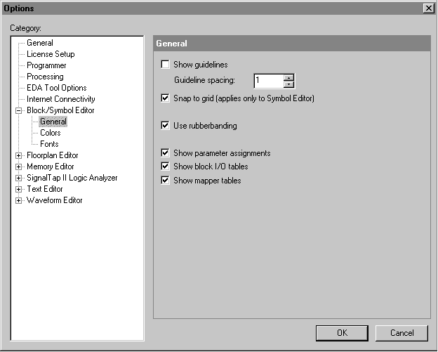
To modify the colors of screen elements and fonts used in the Block Editor window, in the Category list, select Colors or Fonts. Turn appropriate settings on or off in corresponding tabs.
Click OK.
|
You can also view larger or smaller portions of the file with the Zoom Tool, which is available by clicking the Zoom Tool button |
|
To enter input and output pins, follow these steps:
Click the Symbol Tool button ![]() on the toolbar. The same Symbol dialog box that you used to enter the
on the toolbar. The same Symbol dialog box that you used to enter the DFF, DFFE, and mult symbols appears. Note, however, that using the toolbar button opens this dialog box with the Repeat-insert mode option turned on.
| When Repeat-insert mode is turned on, an outline of the selected symbol remains attached to the pointer, regardless of how many times you click the mouse pointer, allowing you to place multiple copies of the symbol easily. Whenever you want to stop placing copies of a symbol, you can press Esc or choose Cancel (right button pop-up menu). |
In the Symbol dialog box, in the Libraries list, click the + icon to expand the d:\quartus\libraries folder, expand the primitives folder, and then expand the pin folder.
In the pin folder, select the input primitive.
Click OK.
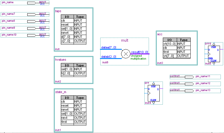
Click an empty space in the BDF five times to insert a total of five INPUT symbols on the left-hand side of the file. Symbols are automatically named as pin_name<number> in sequence. Press Esc.
Repeat steps 1 to 5 to insert and position a total of three OUTPUT symbols on the right-hand side of the file.
![]()
Choose Save (File menu).
|
To name the input and output pins, follow these steps:
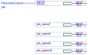
With the Selection and Smart Drawing Tool, double-click the default pin_name pin name of the first input pin symbol you entered.
To rename the pin_name default block name, type clkx2 and press Enter.
| You can also specify the pin name by double-clicking the pin, and then specifying the pin name in the General tab of the Pin Properties dialog box. |
![]()
Repeat steps 1 and 2 to rename each of the pins with the following names:
| Pin Type: | Rename As: | Description: |
INPUT |
clkx2 (already entered) |
Derived clock for the FIR filter. |
INPUT |
clk |
Base clock for the FIR filter. |
INPUT |
d[7..0] |
Data input to the FIR filter. |
INPUT |
reset |
Reset signal for the FIR filter. |
INPUT |
newt |
Input signal that loads the data input d[7..0]
into the taps function. |
OUTPUT |
yn_out[7..0] |
The FIR filter output data. |
OUTPUT |
yvalid |
Indicates that the yn[7..0] filter output
of the acc function is valid. |
OUTPUT |
next |
Indicates that the FIR filter is ready for the next 8-bit data input. |
Move the INPUT and OUTPUT pin symbols so they line up with the appropriate symbols or blocks, as shown in the following illustration:
![]()
Choose Save (File menu).
|
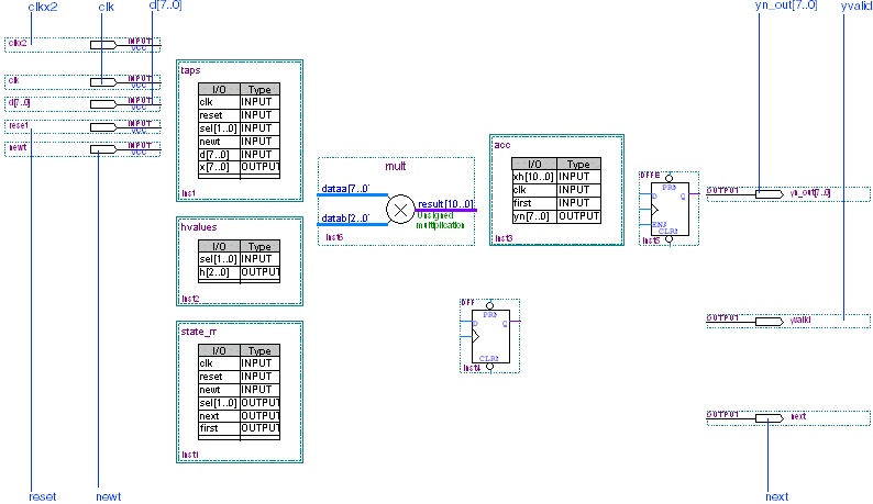
You can use the Selection and Smart Drawing Tool to draw most of the lines you need to connect symbols and blocks in a BDF. The lines that you draw to connect symbols and blocks include nodes, buses, and "conduits." Conduits are hollow lines that represent one or more unordered signals traveling to or from a block.
The Selection and Smart Drawing Tool automatically chooses the appropriate line style when you draw from a symbol pinstub or a block border. For example, it chooses the Orthogonal Node Tool or Orthogonal Bus Tool (depending on the width of the pinstub) when you draw from a symbol pinstub. The Selection and Smart Drawing Tool chooses the Orthogonal Conduit Tool when you draw from a block border. You can also choose a specific line type by clicking the Orthogonal Node Tool, Orthogonal Bus Tool, or Orthogonal Conduit Tool.
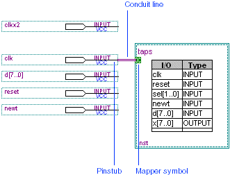
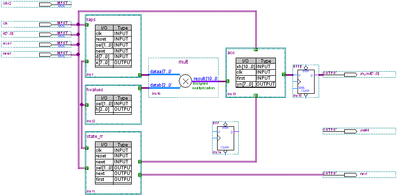
The Quartus II software makes connections automatically between blocks that have been connected together by a conduit. Conduits and signal mapping between blocks are discussed in greater detail later in this tutorial module. The following sections show you how to complete the filtref.bdf file by connecting the symbols and blocks, as shown in the following completed schematic:
![]()

|
To draw conduit lines between symbols and blocks, follow these steps:
Click the Orthogonal Conduit Tool button ![]() on the toolbar.
on the toolbar.
Click the pinstub of the clk input pin to define the start of the conduit, and then drag the pointer to draw a line that connects to the border of the taps block. A "mapper" symbol appears automatically on the edge of the taps block where the conduit connects to the block. A mapper allows you to map I/O port(s) in the block to signal(s) in the conduit. Block mappers are discussed in greater detail later in this tutorial module.
![]()
Repeat steps 1 through 2 to make the additional connections between the symbols and blocks shown in the following table.
| To draw a line that connects a node, bus, or conduit to an existing node, bus, or conduit, you can choose the appropriate Orthogonal Node Tool, Orthogonal Bus Tool, or Orthogonal Conduit Tool button on the toolbar. When you draw a line that connects a node, bus, or conduit to an existing node, bus, or conduit, a connection "dot" appears. |
| Draw Conduit From: | To: |
INPUT pin clk |
taps block (already entered) |
Conduit connecting INPUT pin clk to taps
block |
state_m block |
INPUT pin d[7..0] |
Conduit connecting taps block to state_m block |
INPUT pin reset |
Conduit connecting taps block to state_m block |
INPUT pin newt |
Conduit connecting taps block to state_m block |
taps block |
hvalues block |
Conduit connecting INPUT pin clk to taps block |
acc block |
![]()
|
To view the properties of a conduit, follow these steps:
Click the Selection and Smart Drawing Tool button on the toolbar.
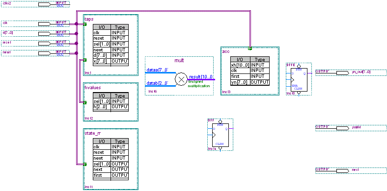
Select the conduit that connects the INPUT pin clk to the taps block, and choose Properties (right button pop-up menu). The Conduit Properties dialog box appears.
Click the Signals tab. The Connections list shows the signal connections for the selected conduit.
![]()
Make sure the signals are correct, and then click OK.
|
To make connections between symbols and blocks using the Selection and Smart Drawing Tool, follow these steps:
Click the Selection and Smart Drawing Tool button on the toolbar.
Draw a line from the conduit that connects the taps block to the hvalues block to the border
of the state_m block. The Selection and Smart Drawing Tool automatically chooses the conduit line style.
Repeat steps 1 through 2 to make the additional conduit connections between the symbols and blocks shown in the following table:
| Draw Conduit From: | To: |
Conduit connecting taps block to hvalues
block |
state_m block (already entered) |
state_m block |
acc block |
state_m block |
OUTPUT pin next |
Repeat steps 1 through 2 to make the bus connections between the symbols and blocks shown in the following table. The Selection and Smart Drawing Tool automatically chooses the bus line style.
| Draw Bus From: | To: |
taps block |
dataa[7..0] input of mult symbol |
hvalues block |
datab[2..0] input of mult symbol |
result[10..0] output of mult symbol |
acc block |
![]()

|
To continue making bus connections, follow these steps:
Click the Orthogonal Bus Tool button ![]() on the toolbar.
on the toolbar.
Draw a bus line from the border of the acc block to the D input of the DFFE symbol.
Repeat steps 1 through 2 to make the additional bus connections between the symbols and blocks shown in the following table:
| Draw Bus From: | To: |
acc block |
D input of the DFFE symbol (already entered) |
Q output of DFFE primitive |
OUTPUT pin yn_out[7..0] |
![]()
|
To draw the appropriate node lines, follow these steps:
Click the Orthogonal Node Tool button ![]() on the toolbar.
on the toolbar.
Draw a node line from the D input of the DFF symbol
to the border of the state_m block.
Repeat steps 1 through 2 to make the additional node connections shown in the following table:
| Draw Node From: | To: |
D input of the DFF symbol |
border of the state_m block (already entered) |
Q output of DFF primitive |
OUTPUT pin yvalid |
INPUT pin clkx2 |
clock input of the DFFE primitive |
enable (ENA) input of the DFFE
primitive |
Node connecting the Q output of the DFF
primitive to the OUTPUT pin yvalid |
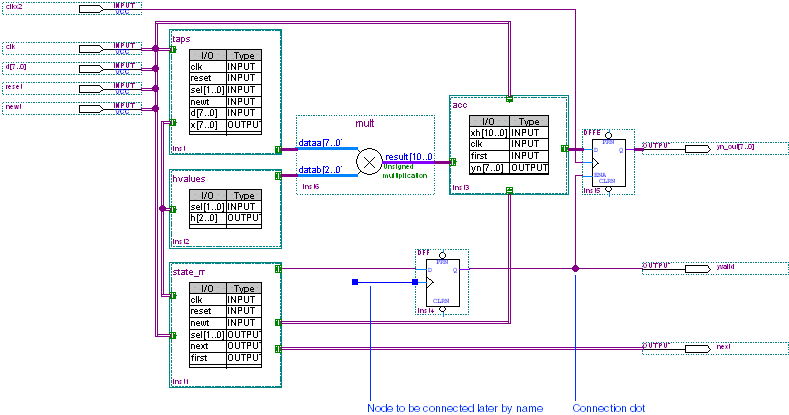
To create a node that can be connected by name, draw a line from the DFF
symbol's clock input into an empty space. You can learn how to complete this node's
connection by name later in this tutorial module.
![]()
Choose Save (File menu).
|
The Quartus II software offers different ways to map signals between blocks and symbols:
| Mapping Method: | Description: |
| "Smart" mapping | If the I/O signal names in one block are the same as in another block, the common I/Os between the blocks are connected automatically in a conduit. You do not need to label these conduits. To prevent an automatic mapping, you can specify that a particular block's I/O port should be mapped to "nothing." |
| Assigning names to nodes or buses (including "connection by name") |
If the I/O names are different between the blocks or symbols you want to connect, you can assign a name to the node or bus that matches the name of one of the block's I/O ports to establish a mapping between that port and the node or bus. Assigning a name is especially useful if you want to connect a conduit to another conduit, even though those conduits are not physically connected. To create a mapping between these conduits and their blocks, you must first make sure that each conduit is connected to a block on one end, but is physically unconnected to any other block or symbol. If you then assign matching names to both conduits (assuming that those names also match I/O ports in the connected blocks), you can establish a "connection by name" between the two conduits and their blocks. You can also use a similar method to connect two nodes by name. |
| Using "mappers" to specify mappings explicitly | If the I/O names are different in the blocks you want to connect, and the blocks are physically connected by a conduit, you can specify the mappings explicitly. You can map the block I/O name to a signal on the conduit and map that signal to the block I/O name you want to connect. |
|
The following table explains which signals in the filtref.bdf design are connected by the Quartus II software automatically through "smart" mapping. The following connections make use of "smart" block mapping—you do not need to explicitly name these connections:
| From: | To: |
INPUT pin clk |
Block I/Os named clk in blocks that are connected
to the clk pin |
INPUT pins d[7..0] |
Block I/Os that are named |
INPUT pin reset |
Block I/Os named reset in the taps and state_m blocks |
INPUT pin newt |
Block I/Os named newt in the taps and state_m blocks |
Block I/O named sel[1..0] in the taps block |
Block I/Os named sel[1..0] in the hvalues and state_m blocks |
Block I/O named first in the state_m block |
Block I/Os named first in the acc block |
Block I/O named next in the state_m block |
OUTPUT pin next |
|
This procedure shows how to map a total of six signals that are not mapped automatically. You first assign appropriate names to two signals in order to establish connections by name. Next, you specify explicit mappings for four other signals.
To assign appropriate names to some of the signals so they can be logically connected, follow these steps:
With the Selection and Smart Drawing Tool, select the node that connects the state_m block to the D input of the DFF primitive.
Choose Properties (right button pop-up menu). The General tab of the Node Properties dialog box appears automatically.
In the Name box, type next as the name of the node.
![]()
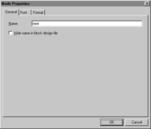
Click OK. The signal next is added automatically to the node, and the name appears above the node line. Adding this name creates a logical connection between the state_m block and the D input of the DFF primitive.
Follow steps 1 through 4 to name the node that feeds the Clock input of the DFF primitive. Name the node clk, so that you can create a logical connection, or a "connection by name," from the INPUT pin clk to the Clock input of the DFF primitive.
Choose Save (File menu).
|
You must now map four other connections explicitly so that the Quartus II software can properly connect the mult symbol to other blocks in the file.
To map other connections between I/O signals in blocks to differently named I/O signals in other blocks, follow these steps:
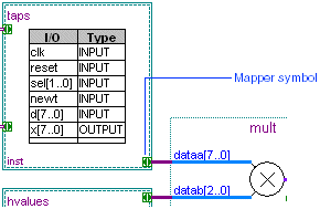
On the bus that connects the taps block to the dataa[7..0] input on the mult symbol, double-click the mapper symbol at the end of the bus on the taps block.
![]()
When you double-click the mapper symbol, the General tab in the Mapper Properties dialog box appears automatically.
In the Type list, select OUTPUT.
![]()
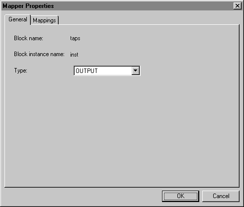
Click the Mappings tab.
In the I/O on block list, select x[7..0].
In the Signals in bus box, type dataa[7..0].
To map the connection, click Add. The mapping appears in the Existing mappings list.
![]()
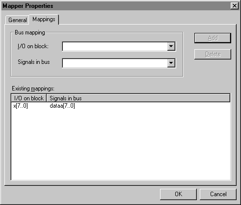
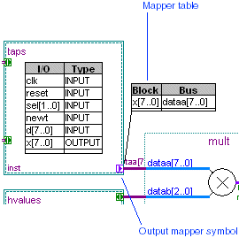
Click OK. The signal dataa[7..0] is added to the bus, and a mapper table appears that shows the mapping information. This mapping is necessary to indicate which signals should feed the dataa[7..0] input port of the mult symbol.
![]()
|
Follow these steps to continue mapping connections between I/O signals in blocks to differently named I/O signals in other blocks:
Repeat steps 1-7 described in Step 7: Map Signals Explicitly to map the connections listed in the following table:
| Connection: | Type: | I/O on Block: | Signals in Bus: |
Bus from the taps block to the dataa[7..0]
input of the mult symbol (already entered) |
OUTPUT |
x[7..0] |
dataa[7..0] |
Bus from the hvalues block to the datab[2..0]
input of the mult symbol |
OUTPUT |
h[2..0] |
datab[2..0] |
Bus from the result[10..0] output of the mult
symbol to the acc block |
INPUT |
xh[10..0] |
result[10..0] |
Bus from the acc block to the D
input of the DFFE primitive |
BIDIR |
yn[7..0] |
yn[7..0] |
![]()
Choose Save (File menu). The BDF is complete.
|
Now that you have created the blocks, you need to create the design files that the blocks represent. You can automatically create a design file that contains the basic framework for the block that represents it. You can then fill in the framework with the design details.
| If you are already familiar with Verilog HDL design entry using the Quartus II Text Editor, you can reduce the time required to complete this tutorial by following the instructions in Copying Altera-Provided Design Files, rather than creating the files from scratch. |
|
To create the framework of a Verilog Design File for the hvalues block, follow these steps:
Select the hvalues block.
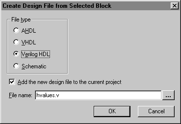
Choose Create Design File from Selected Block (right button pop-up menu). The Create Design File from Selected Block dialog box appears.
Under File type, select Verilog HDL.
Make sure Add the new design file to the current project is turned on.
Make sure the File name box shows the hvalues.v file in the fir_filter project directory.
![]()
Click OK. The Quartus II software confirms that the file has been generated successfully and automatically opens a Text Editor window that contains the new file. The Quartus II software generates the file shown below, which includes a template for a module declaration containing port declarations that correspond to the data you entered in the block:
![]()
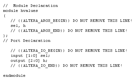
You may notice a few pairs of Quartus II-generated comments that start with "ALTERA" and end with "DO NOT REMOVE THIS LINE!" The Quartus II software updates the information between these pairs of comments, so you must not enter text between them. However, you can enter other Verilog HDL statements outside these commented sections. |
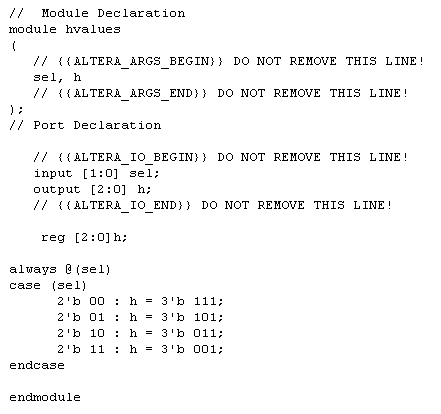
Add the following lines to the hvalues.v file to implement the design. Insert these lines just before the endmodule statement:
reg [2:0]h;

always @(sel)
case (sel)
       	2'b 00 : h = 3'b 111;
       	2'b 01 : h = 3'b 101;
       	2'b 10 : h = 3'b 011;
       	2'b 11 : h = 3'b 001;
endcase
![]()
Choose Save (File menu).
To close the Text Editor, choose Close (File menu).
|
You can copy the Verilog Design Files that are provided for the taps, state_m, and acc blocks.
To copy the taps.v, state_m.v, and acc.v files from the \qdesigns\tutorial subdirectory into the \qdesigns\fir_filter subdirectory, follow these steps for each file:
Choose Open (File menu). The Open dialog box appears.
In the Files of type list, select Device Design Files.
In the \qdesigns\tutorial subdirectory, select the taps.v, state_m.v, or acc.v Altera-provided file in the Files list.
Click Open.
Choose Save As (File menu). The Save As dialog box appears.
In the Save in list, select \qdesigns\fir_filter as the target directory.
Make sure Add file to current project is turned on.
Click Save.
Repeat these steps for each file.
|
The design file acc.v requires a 12-bit adder function, which you can implement with a variation of the lpm_add_sub function. The acc.v file instantiates this function as accum. You can create this custom variation with the MegaWizard Plug-In Manager.
| If you are already familiar with using the MegaWizard Plug-In Manager, you can copy the Altera-provided files that would be generated by the MegaWizard Plug-In Manager, rather than actually generating the files, by following the instructions in Copying Altera-Provided Design Files. |
|
To create a custom Verilog HDL version of the lpm_add_sub function with the MegaWizard Plug-In Manager, follow these steps:
Choose MegaWizard Plug-In Manager (Tools menu). The first page of the MegaWizard Plug-In Manager appears.
![]()
In the first page of the MegaWizard Plug-In Manager, make sure Create a new custom megafunction variation is selected and click Next.
Under Which megafunction would you like to customize?, click the + icon to expand the arithmetic folder, and then select LPM_ADD_SUB.
Specify the following responses to the remaining wizard prompts:
| Wizard Prompt: | Response: |
| Which device family will you be using? | APEX20KE |
| Which type of output file do you want to create? | Verilog HDL |
| What name do you want for the output file? | d:\qdesigns\fir_filter\accum.v |
| How wide should the 'dataa' and 'datab' input buses be? | 12 |
| Which operating mode do you want for the adder/subtractor? | Addition only |
| Is the 'dataa' or 'datab' input bus value a constant? | No, both values vary |
| Do you want any optional inputs or outputs? | Make sure all options are turned off |
| Do you want to pipeline the function? | No |
Click Finish. The wizard creates the accum.v file, and the file is ready to be imported into your project.
|
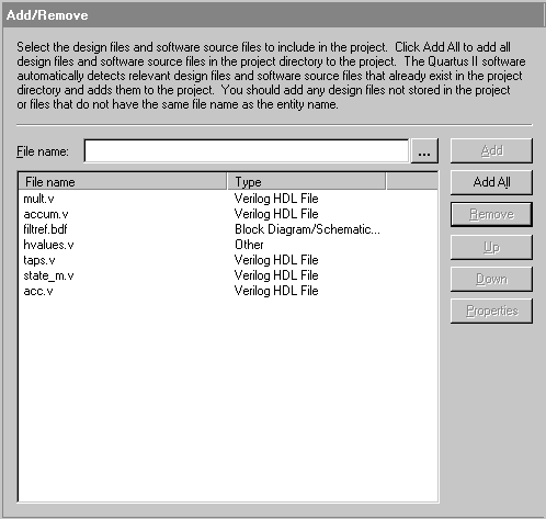
To add the accum.v and mult.v files to the fir_filter project, follow these steps:
Choose Add/Remove Files in Project (Project menu). The Add/Remove page of the Settings dialog box appears automatically.
In the File name box, type accum.v file or select the file with Browse (...). Click Add.
If you have not already added the mult.v file to the project, repeat step 2 to add the file to the project.
![]()
Click OK. You have now created and added all of the necessary design files for the fir_filter project.
|