For Printing Purposes Only! |
|
Click the Print icon to print this Module. Click the Done or Previous button when finished. |
Compilation Module |
The Quartus II Compiler consists of a series of modules that check the design for errors, synthesize the logic, fit the design into an Altera device, and generate output files for simulation, timing analysis, and device programming.
The Compiler first extracts information that defines the hierarchical connections between a project's design files and checks the designs for basic design entry errors. Then, it creates an organizational map of the design and combines all design files into a flattened database that can be processed efficiently.
You can instruct the Compiler to apply a variety of techniques, such as timing-driven compilation, to increase the speed of your design and optimize the device resource usage. Both during and after compilation, you can view the results in the Compilation Report window. The Compiler also creates programming files that the Quartus II Programmer or another industry-standard programmer can use to program or configure an Altera device.
The Compilation tutorial module guides you through the steps necessary to specify Compiler settings, create a resource assignment, compile the top-level design entity, view the fit in the Last Compilation floorplan, assign logic to an Embedded System Block (ESB), and recompile the design.
|
If you did not already create the fir_filter design as described in the Design Entry tutorial module, you must first open the compilation project before you can begin working in the Compilation tutorial module.
To open the compilation project, follow these steps:
Choose Open Project (File menu). The Open Project dialog box appears.
In the \qdesigns\fir_filter\compile subdirectory, select the Altera-provided compile_fir_filter.quartus project file in the Files list.
Click Open.
|
The Quartus II software allows you to compile an entire design, or to compile any constituent part of a design. The "compilation focus," which is the design entity you want to compile, can be selected from any portion of a project's hierarchy.
When you create a new project, the Quartus II software creates default Compiler settings that specify the compilation focus, the type of compilation to perform, the device to target, and other options.
You can also create your own customized Compiler settings for specifying these options. You can switch between different Compiler settings when you compile a design.
| The procedures in this session explain how to view and edit Compiler settings using the Settings dialog box (Assignments menu). However, you can also specify Compiler settings by following the steps in the Compiler Settings Wizard (Assignments menu). |
|
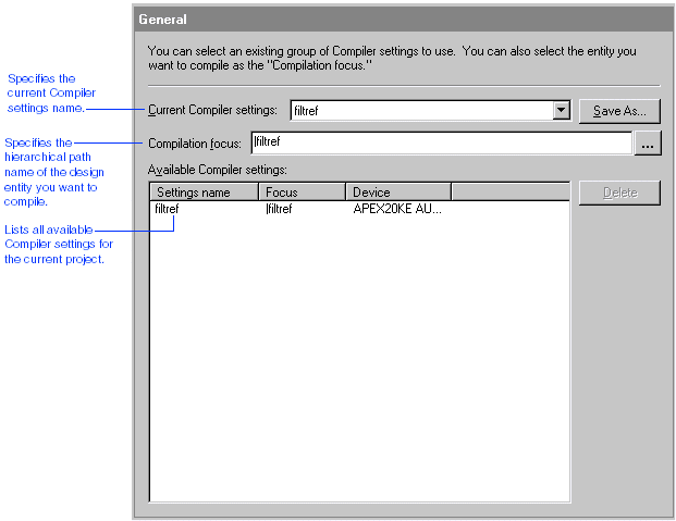
The General Compiler settings page allows you to select an existing group of Compiler settings for use during compilation, define and save a new group of Compiler settings, specify the compilation focus, and delete existing settings.
To view the default Compiler general settings created for the current project, follow these steps:
Choose Settings (Assignments menu). The Settings dialog box appears.
In the Category list, select General under Compiler Settings. The General page appears.
At this point in the tutorial, the General page displays only the default settings created by the Quartus II software when the project was initially created. These default settings are given the name of the top-level design entity in the project, filtref.
![]()
|
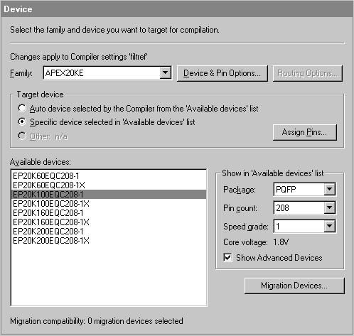
The Device Compiler settings page allows you to select the target device.
To select the target device, follow these steps:
In the Settings dialog box, select Device under Compiler Settings. The Device page appears.
In the Family list, make sure APEX20KE is selected. Click Yes if you are asked whether you want to allow the Quartus II software to select a device and remove any pin assignments.
Under Target device, select Specific device selected in "Available devices" list.
Under Show in "Available devices" list, select the following options:
In the Package list, select PQFP.
In the Pin count list, select 208.
In the Speed grade list, select 1.
In the Available devices list, select EP20K100EQC208-1.
![]()
|
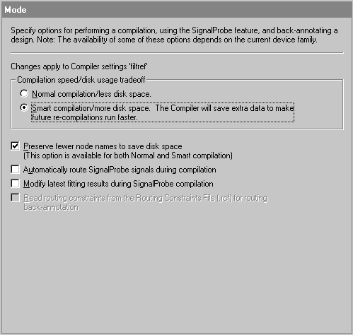
The Mode Compiler settings page allows you to specify options that affect compilation speed, the amount of disk space used for compilation, the SignalProbe feature, and other options.
To specify the Compiler mode settings, follow these steps:
In the Settings dialog box, select Mode under Compiler Settings. The Mode page appears.
To make subsequent recompilations run faster, under Compilation speed/disk usage tradeoff, select Smart compilation/more disk space.
Make sure the Preserve fewer node names to save disk space option is turned on.
![]()
|
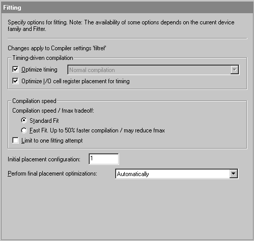
The Fitting Compiler settings page allows you to specify options that control device fitting. You can turn on options in this dialog box to direct the Fitter to optimize the placement of logic in order to meet your timing goals.
To specify Compiler fitting settings, follow these steps:
In the Settings dialog box, select Fitting under Compiler Settings. The Fitting page appears.
Under Timing-driven compilation, turn on Optimize timing, and Optimize I/O cell register placement for timing, and make sure Normal compilation is selected in the list.
Under Compilation speed, make sure Standard Fit is selected.
![]()
In the Settings dialog box, click OK. All of the settings and options you specified are saved as the filtref Compiler settings. When you run the Compiler, these Compiler settings will control compilation processing.
|
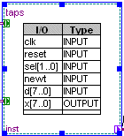
You can assign the logic in your design to specific device resources. For example, you can assign the logic of a block in a Block Design File (.bdf) to a specific MegaLAB™ row in a device. MegaLABs are large-scale structures within APEX™ 20K, APEX II, and ARM®-based Excalibur™ devices. To assign the logic of the taps block to the first row (that is, row A) in the device, follow these steps:
To open to the filtref.bdf block diagram, choose Open (File menu). The Open dialog box appears.
In the Files of type list, select Device Design Files.
In the Files list, select filtref.bdf.
Click Open.
In the filtref.bdf block diagram, select the taps block.

Choose Assignment Organizer (right button pop-up menu). The Assignment Organizer dialog box appears, with the Edit specific entity & node settings for option selected, and with the hierarchical path name of the taps block shown in the Name box.
![]()
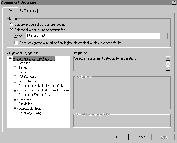
In the Assignment Categories list, click the + icon to expand Locations.
Under Locations, click MegaLAB row.
Under Assignment, select A in the MegaLAB row name list.
In the Zone list, make sure Whole row is selected.
Click Add. The assignment appears in the Assignment Categories list.
Click OK. The logic of the taps block is assigned to row A in the device.
To close the filtref.bdf file, choose Close (File menu).
|
During compilation, the current Compiler settings control design processing. The Compiler automatically locates and uses all non-design files associated with the current compilation focus, such as Include Files (.inc) containing AHDL Function Prototype Statements; Memory Initialization Files (.mif) or Hexadecimal Intel-format Files (.hex) containing the initial content of memories; and Project, Entity, and Compiler Settings Files (.psf, .esf, and .csf) containing project and setting information. During compilation, the Compiler generates information, warning, and error messages that appear automatically in the Messages window.
|
To compile the filtref design entity, follow these steps:
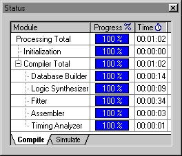
Choose Start Compilation (Processing menu).
The Compiler immediately begins to compile the filtref design entity, and all of its subordinate design entities, using the filtref Compiler settings. As the design compiles, the Status window automatically displays, as a percentage, the total compilation progress and the time spent in each stage of the compilation.
![]()
The results of the compilation are updated in the Compilation Report window. The Compiler runs in the background, freeing your computer—and other portions of the Quartus II software—for other work. However, the compilation of this design entity is short and you should not have to wait long for it to finish.
If you receive a message indicating that compilation was successful and there are no errors displayed in the Messages window, click OK to close the message box.
| You should correct any errors in your design and recompile it until it is error-free before proceeding with the tutorial. If the Compiler displays any error messages in the Messages window, select the message and choose Locate (right button pop-up menu) to find its source(s), and/or choose Help (right button pop-up menu) to display help on the message. |
|
During compilation, all compilation messages appear in the Processing tab of the Messages window. Some messages that appear in the Messages window can be located in a design file or other source file.
To locate the source of a Compiler-generated message, follow these steps:
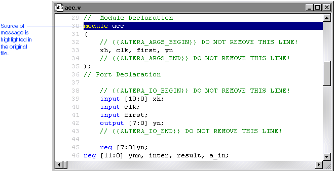
In the Messages window, click the + icon to expand the Found 1 design units and 1 entities in source file D:\qdesigns\fir_filter\<module directory>\acc.v information message.
![]()
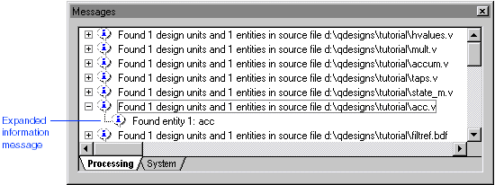
Double-click the Found entity 1: acc expanded information message. The acc.v file, which contains the message source, appears in a Text Editor window, and the section that is the source of the message—the Module Declaration—is highlighted in the file.
![]()
Once you have finished viewing the source of the message, close the Text Editor window.
|
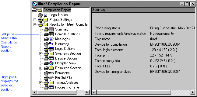
During compilation, the Compilation Report window appears automatically. The Compilation Report provides detailed information about the current compilation. When the report first opens, the Summary section appears in the right pane of the window. This section provides the following information about the compilation:
The final status of the compilation.
The timing requirements, if any.
The name of the design entity compiled.
The total number of logic cells, pins, memory, and PLLs used in the device.
The Compilation Report's other sections provide information about the implementation of the design in the current device, including the following information:
A floorplan showing how the Compiler placed logic in the device.
Detailed device resource usage.
Detailed timing information.
The minimized equations for all logic in the design.
The time required to process the design.
|
To view any section of the Compilation Report, follow these steps:
In the left pane of the Compilation Report window, click the + icon to expand any Report window folder.
![]()
In the left pane of the Report window, select the Report section you want to open. The report appears in the right pane of the window.
| You can go to "Overview: Viewing the Results of a Compilation or Simulation in the Report Window" in Quartus II Help for more information about the Report window. | |
|
The Quartus II software offers three views of a design's floorplan:
The Current Assignments floorplan allows you to edit the location assignments of resources on the device.
The non-editable Last Compilation floorplan shows how the Compiler implemented the design in a device.
The Timing Closure floorplan unifies the Last Compilation and Current Assignments floorplans, which helps you to create effective LogicLock™ regions to enable faster design timing closure.
The Current Assignments and Last Compilation floorplans allow you to view information organized by interior logic cells, interior LABs, interior MegaLAB structures, and the device package top and bottom. The Timing Closure Floorplan is described in greater detail in the LogicLock tutorial module.
|
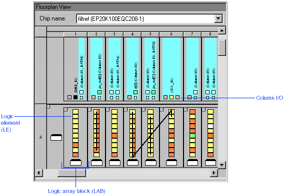
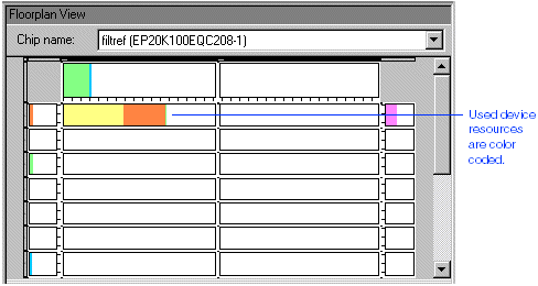
After a successful compilation, you can view the results in the Last Compilation floorplan. The Last Compilation floorplan shows how the Compiler implemented the logic of a design into an Altera device.
To open the Last Compilation floorplan, follow these steps:
Choose Last Compilation Floorplan (Assignments menu). By default, the Interior Cells view of the Floorplan Editor appears, showing the individual logic cells in each LAB. By default, unused logic cells are shown in white. Used logic cells are color-coded to reflect the interconnect used in fitting.
![]()
| You can click and drag the borders of the Floorplan Editor window to resize the window as neccessary. |
To display the color legend, choose Color Legend Window (View menu).
|
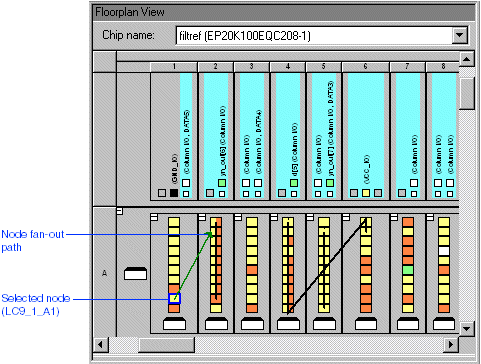
To show node fan-in and fan-out, follow these steps:
Choose Routing > Show Node Fan-Out (View menu).
Select any one of the used logic cells in the floorplan. By default, the the fan-out is shown in green. The arrows in the fan-out lines indicate the direction of the signal flow.
![]()
To display the routing delays, choose Routing > Show Routing Delays (View menu). The routing delays associated with the selected logic cell appear in the floorplan alongside the fan-in and fan-out paths.
When you are finished viewing the fan-in and fan-out paths, turn off Routing > Show Node Fan-Out (View menu).
|
The Equations window allows you to view the equations, fan-in, and fan-out for a selected pin or cell. The Equations window appears automatically at the bottom of the Floorplan Editor window.
To view the equations for the reset input pin, follow these steps:
If necessary, to display the Equations window, choose Equations (View menu).
Select any of the input pins located on the periphery of the device in the Last Compilation floorplan. The Equations window displays the equation for the selected pin. The Fan-Out list displays the node(s) fed by the pin.
![]()
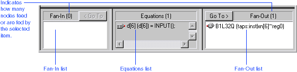
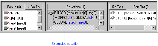
To expand the equation associated with one of the nodes, follow these steps:
At the top of the Fan-Out list, select one of the node names.
Click Go To >. The equation for the selected node appears in the Equations list.
In the Equations list, click the first equation term highlighted in blue. The equation term expands to reveal the substituted equation.
![]()
|
You can view the interior MegaLAB structures of the device in the floorplan. Each MegaLAB contains a number of LABs, one ESB, and a MegaLAB Interconnect structure.
To display the MegaLABs of the device in the Floorplan Editor window, follow these steps:
Choose Interior MegaLABs (View menu). The Floorplan Editor displays the MegaLABs in the device. Unused resources are shown in white, by default. Used resources are color-coded to reflect the interconnect used in fitting.
![]()
In column 1 row A, click the + icon to expand MegaLAB_A1. The MegaLAB expands to show its individual LABs.
Choose Interior Cells (View menu).
After you are finished looking at the Last Compilation floorplan, choose Close (File menu).
|
You can use the Technology Mapper logic option to force the Quartus II software to implement the logic of a design entity into specific device resources, such as ESBs. ESBs are structures within APEX 20K, APEX II, ARM-based Excalibur, and Mercury™ devices, that you can use to implement memory (RAM, ROM, FIFO, or CAM) or combinatorial logic. After making the logic option assignment, you can verify its implementation in the floorplan.
|
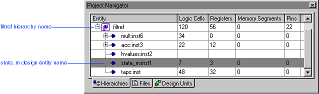
To assign the state_m:inst1 design entity to ESB product term logic, follow these steps:
In the Project Navigator, click the Hierarchies tab.
| The Project Navigator appears by default when you start the Quartus II software. However, if necessary, you can display the Project Navigator by turning on Utility Windows > Project Navigator (View menu). |
In the Hierarchies tab, click the + icon to expand the filtref hierarchy.
In the filtref hierarchy, select the state_m:inst1 design entity name.
![]()
Choose Assignment Organizer (right button pop-up menu). The Assignment Organizer dialog box appears, with the Edit specific entity & node settings for option selected, and with the hierarchical path name of the state_m:inst1 entity shown in the Name box.
In the Assignment Categories list, click the + icon to expand Options for Entities Only.
Click the Click here to add a new assignment text.
Under Assignment, in the Name list, select Technology Mapper -- APEX 20K/20KE/20KC/APEX II/ARM-based Excalibur.
In the Setting list, select Product Term.
![]()
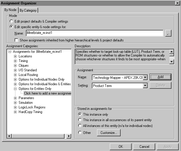
Click Add. The logic option assignment appears in the Assignment Categories list.
Click OK.
|
To recompile the design and implement the new logic option assignment:
Choose Start Compilation (Processing menu).
When you receive a message indicating that compilation was successful, click OK to close the message box.
|
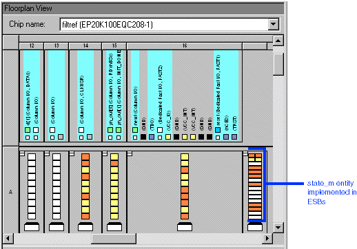
To view the implementation of the logic option assignment in the Last Compilation floorplan, follow these steps:
Choose Last Compilation Floorplan (Assignments menu).
If necessary, click the Selection and Smart Drawing Tool button ![]() on the toolbar.
on the toolbar.
With the Selection and Smart Drawing Tool, point to some of the used ESBs, located at the center of row A. The names of the signals appear in "bubble text." The signal names all start with "state_m," indicating that the logic of the state_m entity is implemented in the ESBs.
![]()
|